"Pick and Place" assembly of parts using PDMS - Amy Lim
What is PDMS?

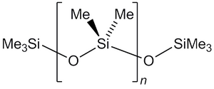
Polydimethylsiloxane (PDMS) is a silicone elastomer, being the simplest kind of silicone polymer at that. [1] PDMS is made up of a monomer and crosslinker curing agent. [2] Often combined at a weight ratio of 10:1, the PDMS mixture undergoes a process of degassing and curing to harden. [2] Changing the ratios of monomer and curing agent offers control over different properties, changing mechanical, optical, and permeability. [2] PDMS has incredible chemical and physical properties that allow for ease of microfluidic device creation. Such properties include being chemically inert (unreactive), thermodynamically inert, easy to handle and manipulate, and less expensive than pure silicone. [3] PDMS has elastomeric properties that allow for its use in soft lithography for techniques such as soft lithography for micro-contact printing, replica molding, and micro-transfer molding just to name a few. [3] PDMS is especially useful in the development of biomedical devices, due to its inherent optical transparency, nontoxicity, and biocompatibility. [3]
Microfludic Device Assembly Methods
Traditional Microfluidic Device Assembly
Microfluidic devices are traditionally assembled one at a time through a wide variety of approaches. These approaches can be integrated, modular, or hybrid. [4] The integrated method approaches assembly as a single, integrated process for the whole device. [4] Although initially well-organized, component parts cannot be individually perfected for use in different, specific applications. [4] Alternatively, modular approaches offer more control over individual component parts of devices. Modular assembly is well known in the processing of microfluidic circuit boards and for Lab-on-Chip technologies. [4] Modular devices may be assembled through the stacking of microscale layers, the embedding of components, and the use of cartridges. [4] Modular assembly leads way for another method of microfluidic device assembly called "Pick and Place."

"Pick and Place" Assembly
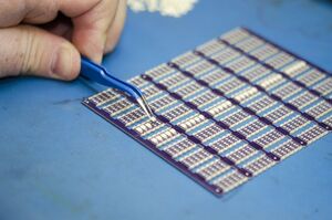
Conventional "Pick and Place" (PNP) assembly is often seen in the assembly of electronic parts through robotic assistance. [5] PNP assembly is exactly how it sounds: premade components are placed in predetermined ways to increase manufacturing efficiency. [5] PNP machines are often employed to assemble many devices at once. The PNP assembly method is very similar to conveyer belt manufacturing at a large factory. Many PNP machines have vacuum-assisted parts that are used to "pick" specific components and "place" them in their correct space and orientation. [5] PNP assembly is much more efficient compared to simple modular assembly, as it automates an existing assembly process into a much faster and more efficient one. PDMS can also be used in PNP assembly for especially fragile component parts with their adhesive and elastomeric properties. [6]
"Pick and Place" Microfluidic Device Assembly with PDMS
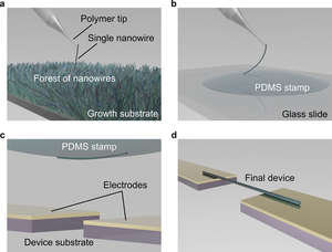
Due to its ability to carefully "pick" up tiny component parts and "place" them in specific locations without much prior handling, PDMS-based assembly is a great alternative to vacuum-based part assembly. PDMS' mechanical properties allow PDMS stamps to adhere to particular components based on strain energy and interface toughness characteristics. [6] Viscoelastic (viscosity and elasticity) properties of PDMS stamps control which parts will be picked up for placement. With PDMS, different ratios of monomer and crosslinker agents are used to adhere to different components of different viscoelastic properties. [6] Additionally, the viscoelastic properties of PDMS allow for novel transfer-printing technologies for Micro-Electro-Mechanical systems (MEMS), which may be useful in large-scale lithography procedures. [6]
Applications of "Pick and Place" Assembly with PDMS
As described before, PDMS-based "Pick and Place" assembly has a wide variety of applications, including those of biological simulation and nanoscale materials.
Organ-on-Chip
Methods for "Pick and Place" assembly and transfer of PDMS membranes Organ-on-Chip have been developed for reliability and ease. [7] Instead of the conventional PDMS stamp mentioned prior, the Organ-on-Chip attaches to the "Pick and Place" mechanism through the device's PDMS components. Organ-on-Chip devices simulate the microstructures of various organs in replicated in vivo conditions, which can be used to better understand bodily processes and replace animals in drug development. [7] Such devices are made of PDMS and are fabricated through 3D printing and soft lithography. [7] PDMS is used for its permeability and strong structural characteristics in Organ-on-Chip devices. [7] Membranes as small as a few microns must be transferred reliably and without damage. [7] To transfer Organ-on-Chip devices, porous PDMS membrane layers were developed on the device itself and the surface of the carrier wafer. [7] The PDMS portions are treated with polyacrylic acid and oxygen plasma to bond at constant pressure. [7] The bonding region properties of the two component parts can be changed accordingly for each device made. [7] Lastly, water allows the Organ-on-Chip devices to be removed from the carriers with ease, dissolving the polyacrylic acid layer that served as the "glue." [7] The transfer process designed for Organ-on-Chip is easily reproducible for "Pick and Place" automation because surfaces need only be brought into close contact. [7]
Nanowires

As the name suggests, Nanowires are tiny wires that exist on the nanoscale. Nanowires service a variety of applications, including their use as microfluidic channels. Due to their incredible electrical and optical properties, nanowires have a wide range of applications in electrodes, nanophotonic devices, and Transmission Electron Microscopy (TEM). [8] Although nanowires have promising uses in the aforementioned applications, they have not yet been reliably integrated for microfluidic device assembly. [8] Currently, a stamp transfer technique, as described in other sections, has the best potential for nanowire transfer and placement mechanisms. [8] Unfortunately, a lot of the time, nanowire "pick" up is not very precise, as the stamping technique adheres to more nanowires than desired. [8] However, techniques of more precise pick-up are now being developed through intricate understandings of nanomechanical vibrations and field coupling. [8] Complete automation of microfluidic device manufacturing will soon be possible with the further development of universal "Pick and Place" assembly for nanowires.
References
1. Polydimethylsiloxane. https://www.acs.org/molecule-of-the-week/archive/p/polydimethylsiloxane.html (accessed Apr 16, 2023).
2. Miranda, I.; Souza, A.; Sousa, P.; Ribeiro, J.; Castanheira, E. M. S.; Lima, R.; Minas, G. Properties and applications of PDMS for Biomedical Engineering: A Review. https://doi.org/10.3390/jfb13010002.
3. Mata, A.; Fleischman, A. J.; Roy, S. Characterization of Polydimethylsiloxane (PDMS) Properties for Biomedical Micro/Nanosystems. https://doi.org/10.1007/s10544-005-6070-2.
4. Gray, B. Microfluidic Assembly. In: Li, D. (eds) Encyclopedia of Microfluidics and Nanofluidics. https://doi.org/10.1007/978-0-387-48998-8_926.
5. Electronics Assembly. https://learn.sparkfun.com/tutorials/electronics-assembly/pick-and-place#:~:text=A%20pick%20and%20place%20 (accessed Apr 16, 2023).
6. Wu, J.; Dan, Q.; Liu, S. Effect of viscoelasticity of PDMS on transfer printing. https://doi.org/10.1109/ICEPT.2015.7236694.
7. Quiros-Solano, W. F.; Gaio, N.; Silvestri, C.; Arik, Y. B.; Stassen, O. M. J. A.; Meer, A. D. V. D.; Bouten, C. V. C.; Berg, A. V. D.; Dekker, R.; Sarro, P. M. A novel method to transfer porous PDMS membranes for high throughput organ-on-chip and lab-on-chip assembly. https://doi.org/10.1109/MEMSYS.2018.8346550.
8. Ali, U. E.; Yang, H.; Khayrudinov, V.; Modi, G.; Cheng, Z.; Agarwal, R.; Lipsanen, H.; Bhaskaran, H. A Universal Pick-and-Place Assembly for Nanowires. https://doi.org/10.1002/smll.202201968.
