Replica molding (REM) is a form of soft lithography which utilizes materials such as polydimethyl-siloxane to create microfluidic devices through duplication of shape and structure of a mold.[1] REM typically is used to mold patterns with features on a nano-scale (typically ≤100 nm in dimension)[2] that often are too difficult for other forms of molding (i.e. injection molding) to replicate. While there are a few different organic polymers that can be used in the replica molding process, the most commonly used polymer is Poly(dimethyl-siloxane), commonly referred to as PDMS. A wide range of products ranging anywhere from CDs to various biomedical devices are created using Replica Molding.
PDMS
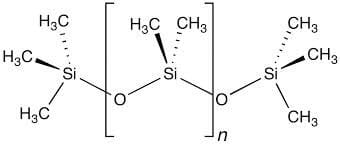
Figure 1. Poly(dimethyl-siloxane) chemical structure.[10]
Poly(dimethyl-siloxane) (PDMS) is a organosilicon organic polymer that has very unique material properties. PDMS is also the most common compound used in soft lithography. Since PDMS is a stiff elastomer (Young's modulus of ~0.5 MPa) and can be high in fidelity, it makes it the perfect compound to mold to some form of previously created structure. It has the ability to conform to nano-scale level of detail required for a microfluidic device.
PDMS is normally hydrophobic but can become hydrophilic when oxidized, allowing it to bind to many different types of molds and substrates by utilizing its ability to shift hydrophobicity. On top of its binding ability, PDMS has key physical properties such as the compound being both transparent and non-toxic: two major benefits for microfluidic devices with biological potential. [3] The first advantage is that due to PDMS's non-toxic nature, it allows for culturing of cells directly on a given device as well as potential for in vivo implantations. The second benefit is due to PDMS's transparent nature, allowing a number of detection schemes to be used on the mold, such as UV absorbance or fluorescence. A characteristic that is both beneficial as well as potentially detrimental, is that PDMS is both gas permeable as well as moderately water permeable. This is a characteristic that entirely depends on the real world application of the PDMS. On an industrial level, PDMS is both very cheap to produce and purchase. When purchased, the package fully comes with the two liquid agents, base, and curing agent, and simply requires mixing and degassing to remove air bubbles to be ready for application.[4]
REM Process
Photolithography for Creation of Master
Replica Molding (REM) takes place once a master for the device is created from rapid prototyping.[5] REM is used as the primary method of channel creation in the molding compound. Before Replica Molding can begin, a silicon wafer is first created coated in photoresist, such as SU 8, and then spun so that the surface of the wafer is totally covered in photoresist. If using a negative photoresist, the photoresist-wafer complex is then heated allowing the formation of a cross-link between the photoresist and the silicon. This cross-linking forms silicon-oxygen bonds (Si-O-Si), which forms tight seals between the silicon wafer and photoresist.
Figure 2. Master creation and REM process flowchart.[4]
A mask made of either plastic or glass is then laid on top of the photoresist-wafer complex and exposed to UV light. Once the UV light is applied, the mask is removed from the photoresist and the whole wafer is submerged in an organic solvent, such as polyethylene glycol, in order to dissolve the portions of the photoresist which had not been cross-linked due to the spaces created by the mask.[3] Once dissolved, the full Master has been formed with the features of the device imprinted into the photoresist.
Molding Process
Before the PDMS is applied to the master, the master undergoes hydrophobic treatment by applying a chemical such as perfluoralkyl trichlorosilane, which prevents the PDMS from sticking to the wafer, which would ruin the device. The PDMS prepolymer is then created and mixed to uniformity and poured onto the master. Once the prepolymer is set onto the master, the prepolymer is either heat treated using an oven or UV treated under a UV lamp, depending on the type of mold and master compounds. Typically the PDMS is heated at somewhere between 60°C-70°C for whatever time it takes for the PDMS to solidify.[1][4] The PDMS is then peeled away from the master and contains a negative embossed image of the master.
Figure 3. REM process: A) Master creation, B) Reservoir and access hole creation, C) Replica molding PDMS cast deployment, D) Negative replica removal, E) Sealing process[1]
One way to form the access wells or holes in order to deploy solution or buffer is by placing posts on the master before application of the PDMS. This allows for the wells to be uniformly formed in the PDMS without having to take an extra step to cut out each hole. Another potential way to form these access wells is through the use of a sharp tool such as a borer to dig down into the mold and excavate a new cavity.
Using the PDMS Stamp to Make the Device
The final step in Replica Molding is creating a device by pouring a UV curable prepolymer over the PDMS, such as polyurethane. Processes like Microcontact Printing or Microtransfer Molding are common ways of creating devices from a PDMS stamp that is created through Replica Molding. Each process utilizes the negative embossing of a PDMS stamp to imprint and copy the desired device design. [4][6]Figure 4. Examples of PDMS to device transfer. A) Replica Molding, B) Microcontact Printing, C) Micromolding, D) Microtransfer Molding.[4]
Advantages of REM
There are a few major advantages to creating molds through Replica molding. The biggest advantage is that you can create 50+ from the creation of one mold from the master. This drastically decreases both spending and time to create specific patterns that would consistently be used in creating various devices. Another major advantage is that REM works with a wide variety of compounds and polymers so that the device can be created specific to the desired compound. The final advantage is that REM can create molds that cover a wide range of surfaces including non-planar curved shapes, and large area masters. Replica molding is a very useful universal pattern replicating technique that can be used for a wide variety of shapes and compounds, without many issues. [1][4][6][7]Figure 5. Valleys molded into PDMS on a 50 x 50 μM2 channel.[1]
Applications of REM
Cell Shaping
Devices created through the use of soft lithography techniques such as REM, are often based in the biological devices. One prime example of REM being used is PDMS channels being created to make hydrogels. These hydrogels can be used for a variety of different types of research but can be used to both grow and pattern cells. For example, if an oval shaped channel is the environment a cell is growing in, it will be physically confined and forced to form the shape of the channel. The cells grown this way can then be dispersed in solution for research.[8]
Sorting of DNA
Another device that has been created using replica molding is a device that sorts DNA by size. [8] The device sorted DNA strand into each channel by size allowing for detection of the amount of each type of strand present in a sample. Due to PDMS being optically transparent, the researchers were also able to read fluorescence levels in the DNA to aid in determining the size.[9]
Flexible Pressure Sensor
In the surging healthcare fields, pressure has become a critical indicator monitored in many biomedical and clinical applications, Figure 6. Microstructured PDMS pressure sensor fabrication.[15]including for cardiovascular disease, intracranial pressure, pulmonary disease, and urinary pressure, through flexible and meanwhile ultra-thin devices.[11] Capacitive sensing, which detects changes in capacitance relative to the pressure applied, is a widely used principal in microsystem based sensors.[12] In general, the device is made up by two conductive electrodes separated by a dielectric medium with designed microstructure to improve sensitivity.[13] Leveraging on its high biocompatibility, elasticity, and easily patterned feature, microstructured PDMS dielectric layer via REM has been utilized to fabricate devices for real time health and rehabilitation monitoring.[14][15]
References
[1] McDonald, J. C.; Anderson, J. R.; Duffy, D. C.; Chiu, D. T.; Wu, H.; Whitesides, G. M. Fabrication of microfluidic systems in Poly(Dimethylsiloxane). Electrophoresis 2000, 27–40. doi: 10.1002/(SICI)1522-2683(20000101)21:1<27::AID-ELPS27>3.0.CO;2-C
[2] Xia, Y.; Mcclelland, J. J.; Gupta, R.; Qin, D.; Zhao, X.-M.; Sohn, L. L.; Celotta, R. J.; Whitesides, G. M. Replica molding using polymeric materials: A practical step toward nanomanufacturing. Adv. Mater. 1997, 9 (2), 147–149. doi:10.1002/adma.19970090211
[3] Qin, D.; Xia, Y.; Whitesides, G. M. Soft lithography for micro- and nanoscale patterning. Nature Protocols 2010, 5 (3), 491–502. doi:10.1038/nprot.2009.234
[4] Weibel, D. B.; Diluzio, W. R.; Whitesides, G. M. Microfabrication meets microbiology. Nat. Rev. Microbiol. 2007, 5 (3), 209–218.doi:10.1038/nrmicro1616
[5] Xia, Y.; Mcclelland, J. J.; Gupta, R.; Qin, D.; Zhao, X.-M.; Sohn, L. L.; Celotta, R. J.; Whitesides, G. M. Replica molding using polymeric materials: A practical step toward nanomanufacturing. Adv. Mater.s 1997, 9 (2), 147–149. doi: 10.1081/E-ENN 120009219
[6]Xia, Y.; Whitesides, G. M. Soft Lithography. Annu. Rev. Mater. Sci. 2010, 29 (25), 153–184. doi:10.1146/annurev.matsci.28.1.153
[7]Mata, A.; Fleischman, A. J.; Roy, S. Characterization of Polydimethylsiloxane (PDMS) Properties for Biomedical Micro/Nanosystems. Biomed. Microdevices 2005, 7 (4), 281–293. doi: 10.1007/s10544-005-6070-2
[8] Heo, J., Thomas, K. J., Seong, G. H. & Crooks, R. M. A microfluidic bioreactor based on hydrogel-entrapped E. coli: Cell viability, lysis, and intracellular enzyme reactions. Anal. Chem. 75, 22–26 (2003). doi:10.1021/ac0259717
[9] Chou, H.-P., Spence, C., Schere, A., Quake, S., Proc. Natl. Acad. Sci. USA 1999, 96, 11±13. PMCID: PMC15083
[10] "PDMS: A Review." Elveflow. Elveflow, 2015. Web. 24 Mar. 2017.
[11]Wen Hsiung, K.; Hynecek, J.; Boettcher, S. F., Development of a miniature pressure transducer for biomedical applications. IEEE T. ELECTRON DEV. 1979, 26 (12), 1896-1905. doi: 10.1109/T-ED.1979.19793
[12]Zhuo, B.; Chen, S.; Zhao, M.; Guo, X., High Sensitivity Flexible Capacitive Pressure Sensor Using Polydimethylsiloxane Elastomer Dielectric Layer Micro-Structured by 3-D Printed Mold. IEEE T. ELECTRON DEV. 2017, 5 (3), 219-223. doi: 10.1109/JEDS.2017.2683558
[14]Huang, Z.; Gao, M.; Yan, Z.; Pan, T.; Khan, S. A.; Zhang, Y.; Zhang, H.; Lin, Y., Pyramid microstructure with single walled carbon nanotubes for flexible and transparent micro-pressure sensor with ultra-high sensitivity. Sens. and Actuators A Phys. 2017, 266, 345-351. doi: 10.1016/J.SNA.2017.09.054
[15]Pignanelli, J.; Schlingman, K.; Carmichael, T. B.; Rondeau-Gagné, S.; Ahamed, M. J., A comparative analysis of capacitive-based flexible PDMS pressure sensors. Sens. and Actuators A Phys. 2019, 285, 427-436. doi: 10.1016/j.sna.2018.11.014


