"Pick and Place" Assembly of Parts Using PDMS - Amy Lim, Rylie Costello
"Pick and Place" Methodology
Overview
"Pick and place" (PNP) assembly is a common mode of manufacturing at both the large and small scales. PNP assembly is exactly how it sounds: premade components are placed in predetermined ways, oftentimes through automation, to increase manufacturing efficiency. Conventional PNP assembly is often seen in the assembly of electronic parts through robotic assistance at both the large and small scale (Video 1).[1] PNP can be done in a variety of ways. There are large production lines that utilize machinery like robotics as well as manual workers to assemble items with this method. When large assembly lines are not used, the pick and place method is skill-dependent and often can entail lots of trial and error.[2] Machines are often employed to assemble many devices at once with high efficiency and accuracy. The PNP assembly method is very similar to conveyer belt manufacturing at a large factory. Many PNP manufacturing lines are equipped with things like vacuum assisted parts to assist the process.[1] PNP assembly is much more efficient compared to simple modular assembly, as it automates an existing assembly process into a much faster and more efficient one.
At the Microscale
PNP is employed at the microscale since many normal manufacturing methods are much harder to apply to such small items. Assembling parts separately and then placing them together allows for much more accurate and rapid assembly of microscale items. However, picking up and releasing items at the microscale is much more difficult due to the strong adhesion forces between the object and the tool being used to place it down.[2] When releasing microscale pieces, there are two main techniques: passive and active release.[2] Passive release relies on the fact that the object can detach from the tool on its own, which is largely dependent on the surface properties of the object, the tool, and the substrate. Passive release is only possible when the interactions between the object and the substrate can naturally overcome the connections to the tool. If they can not, active release methods become useful. Active release is when another force is introduced to detach the object from the tool without touching the substrate.[2] Such techniques include applying an electrical field, mechanical vibration, ice droplets, or vacuum devices (as mentioned above).[2]
Microfludic Device Assembly Methods
Traditional Microfluidic Device Assembly
Microfluidic devices are traditionally assembled one at a time through a wide variety of approaches. These approaches can be integrated, modular, or hybrid.[3] The integrated method approaches assembly as a single, integrated process for the whole device.[3] This includes things like injection molding, surface micromachining, and 3D printing among others. Although integrated methods are initially well-organized, their component parts cannot be individually perfected for use in different, specific applications.[3] Alternatively, modular approaches offer more control over individual component parts of devices. Modular assembly is well known in the processing of microfluidic circuit boards and for Lab-on-Chip technologies.[3] Modular devices may be assembled through the stacking of microscale layers, the embedding of components, and the use of cartridges.[3] Modular assembly is usually combined with fabricating methods like photolithography, soft lithography, micro-contact printing, Modular assembly leads way for another method of microfluidic device assembly called "Pick and Place."
Drawbacks to Traditional Methods
Some drawbacks to traditional microfluidic manufacturing are the time, the necessary precision, and the cost it takes to make one small device. Pick and place assembly can help to mitigate each of these factors. Utilizing tools to assemble pieces one by one increases the precision. Furthermore, through using large-scale pick and place the cost and time necessary to make devices can decrease significantly.[4]
"Pick and Place" and PDMS

What is PDMS?
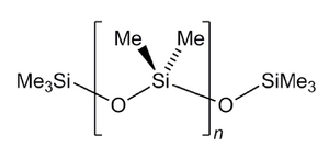
Polydimethylsiloxane (PDMS) is a silicone elastomer, being the simplest kind of silicone polymer at that.[5] PDMS is made up of a monomer and crosslinker curing agent.[6] Often combined at a weight ratio of 10:1, the PDMS mixture undergoes a process of degassing and curing to harden.[6] Changing the ratios of monomer and curing agent offers control over different properties, such as mechanical strength, optical transparency, and permeability.[6] PDMS has incredible chemical and physical properties that allow for ease of microfluidic device creation. Such properties include being chemically inert (unreactive), thermodynamically inert, easy to handle and manipulate, and less expensive than pure silicone.[7] PDMS has elastomeric properties that allow for its use in soft lithography for techniques such as micro-contact printing, replica molding, and micro-transfer molding just to name a few.[7] PDMS is especially useful in the development of biomedical devices, due to its inherent optical transparency, nontoxicity, and biocompatibility.[7]
"Pick and Place" with PDMS
PDMS has strong applications in transfer printing due to its elastomeric properties,[8] and these same benefits can apply to PNP. Due to its ability to carefully "pick" up tiny component parts in substrate and "place" them in specific locations without much prior handling, PDMS-based assembly is a great example of passive-release PNP, avoiding the use of any unnecessary technology or lost precision. PNP assembly with PDMS has been achieved before with several hundred microscale PDMS pillars of 25-35 µm in diameter and 90 µm in height.[9] Experimentally, the several hundred PDMS PNP pillars were able to "pick and place" silicon platelets with the dimensions of 100 x 100 x 3 µm3.[9] The mechanism of "pick and place" assembly can be thought of as a very selective magnet. The intermolecular force interactions between the tip of the PDMS pillar and the surface of the part play a large role in their adhesion and release, with adhesion and contact area having a directly proportional relationship.[9] As a result, to "pick" parts, vertical compression is applied to the tip of the pillar to increase the contact area between the tip and part, which allows for the secure hold of the part that withstanding sudden impacts and disturbances during transfer.[9] On the other hand, to release the part, the contact area of the pillar is greatly reduced via deformation, reducing the overall adhesion of the pillar to the part.[9] With PDMS, different ratios of monomer and crosslinker agents are used to vary the elasticity and stiffness which allows the material to adhere to different components with different surface properties.[10] Contact angle also plays a large role in transfer physics. When the angle between the item being picked up and the surface of the tool decreases, it is easier to release the item because the detachment "crack" can begin propagating from the <90 degree corner that is created.[8] The properties of PDMS to be flexible, slightly adherent, and still maintain microscale features make it so useful in pick and place manufacturing at the microscale.

Biology-Inspired Solution
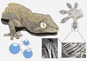
PDMS-based pick and place device assembly is greatly inspired by the controllable attachment and detachment capabilities of the fibrillar structures on gecko feet.[9] Geckos have the ability to selectively adhere to both smooth and rough surfaces by changing the contact area and angles between their feet and surfaces.[9] Mechanically deforming the fibrillar structures changes the contact area between structures and the substrate, which is what causes detachment from a surface.[9] Attaching to a surface is caused by van der Waals interactions between the two surfaces, which is also true for passive pick and place methods.[9] The control over the deformation of their feet fibers gives geckos the ability to be "self-cleaning", meaning they can shed dirt and debris from their feet without wetting.[9] Replicating the properties of self-cleaning and controllable adhesion in a rigid material like the fibrillar structures on gecko feet is desirable with respect to pick and place microfluidics since this method allows for microscale placement of items with accurate, clean adhesion that can easily be broken.[9]
"Pick and Place" for Microfluidics

Nanowires
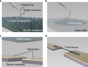
As the name suggests, Nanowires are tiny wires that exist on the nanoscale. Nanowires service a variety of applications, including their use as microfluidic channels. Due to their incredible electrical and optical properties, nanowires have a wide range of applications in electrodes, nanophotonic devices, and Transmission Electron Microscopy (TEM).[11] Although nanowires have promising uses in the aforementioned applications, they have not yet been reliably integrated for microfluidic device assembly.[11] Currently, a PDMS stamp transfer technique, as described in other sections, has the best potential for nanowire transfer and placement mechanisms.[11] A lot of the time, nanowire "pick" up is not very precise, as the stamping technique adheres to more nanowires than desired.[11] However, techniques of more precise pick-up are now being developed through intricate understandings of nanomechanical vibrations and field coupling.[11] Complete automation of microfluidic device manufacturing will soon be possible with the further development of universal pick and place assembly for nanowires.
Cell Manipulation
PDMS grippers have been developed to be used to manipulate individual cells, including picking them up and moving them.[12 ] Although not a device itself, PDMS grippers can be integrated into microfluidic devices because of their small size and accuracy. The PDMS is cast and molded into the shape of a gripper that can squeeze a single cell suspended in liquid.[12 ] One study showed that they were able to pick and place the cell with reliable adhesion and detachment.[12 ] This device exemplifies the versatility of PDMS and shows promise for integrating this technology to other biological objects and microfluidic devices.
MEMS Devices
PDMS stamps have been used as a new way to construct MEMS devices. MEMS devices are micro-electric-mechanical systems that are used for a variety of applications like sensors and actuators.[13] These devices require fragile and complex structures like combs and suspended micro beams that are on the order of microns in size. One paper used PDMS stamps to transfer their microscopic parts to manufacture a MEMS device.[13] The pieces that the silicone stamps were used to pick up and stack on top of one another were as small as 20 µm thick and intricately patterned. Other methods of manufacturing like using grippers or microprobes possess adhesion forces that are too strong for such fragile pieces, or are overly complex.[13] The combination of PDMS based pick and place with the other techniques in this paper like rapid thermal annealing make way for efficient and precise manufacturing of MEMS devices.
References
1. Electronics Assembly. https://learn.sparkfun.com/tutorials/electronics-assembly/pick-and-place (accessed Apr 16, 2023).
2. Y. Zhang; B. K. Chen; X. Liu; Y. Sun. Autonomous Robotic Pick-and-Place of Microobjects. IEEE Transactions on Robotics 2010, 26 (1), 200–207. https://doi.org/10.1109/TRO.2009.2034831.
3. Gray, B. Microfluidic Assembly. In Encyclopedia of Microfluidics and Nanofluidics; Li, D., Ed.; Springer US: Boston, MA, 2008; pp 1136–1147. https://doi.org/10.1007/978-0-387-48998-8_926.
4. Hosic, S.; Bindas, A. J.; Puzan, M. L.; Lake, W.; Soucy, J. R.; Zhou, F.; Koppes, R. A.; Breault, D. T.; Murthy, S. K.; Koppes, A. N. Rapid Prototyping of Multilayer Microphysiological Systems. ACS Biomater. Sci. Eng. 2021, 7 (7), 2949–2963. https://doi.org/10.1021/acsbiomaterials.0c00190.
5. Polydimethylsiloxane. American Chemical Society. https://www.acs.org/molecule-of-the-week/archive/p/polydimethylsiloxane.html (accessed 2024-04-13).
6. Miranda, I.; Souza, A.; Sousa, P.; Ribeiro, J.; Castanheira, E. M. S.; Lima, R.; Minas, G. Properties and Applications of PDMS for Biomedical Engineering: A Review. Journal of Functional Biomaterials 2022, 13 (1), 2. https://doi.org/10.3390/jfb13010002.
7. Mata, A.; Fleischman, A. J.; Roy, S. Characterization of Polydimethylsiloxane (PDMS) Properties for Biomedical Micro/Nanosystems. Biomed Microdevices 2005, 7 (4), 281–293. https://doi.org/10.1007/s10544-005-6070-2.
8. Yang, S. Y.; Carlson, A.; Cheng, H.; Yu, Q.; Ahmed, N.; Wu, J.; Kim, S.; Sitti, M.; Ferreira, P. M.; Huang, Y.; Rogers, J. A. Elastomer Surfaces with Directionally Dependent Adhesion Strength and Their Use in Transfer Printing with Continuous Roll-to-Roll Applications. Advanced Materials 2012, 24 (16), 2117–2122. https://doi.org/10.1002/adma.201104975.
9.Mengüç, Y.; Yang, S. Y.; Kim, S.; Rogers, J. A.; Sitti, M. Gecko-Inspired Controllable Adhesive Structures Applied to Micromanipulation. Advanced Functional Materials 2012, 22 (6), 1246–1254. https://doi.org/10.1002/adfm.201101783.
10. J. Wu; Q. Dan; S. Liu. Effect of Viscoelasticity of PDMS on Transfer Printing. In 2015 16th International Conference on Electronic Packaging Technology (ICEPT); 2015; pp 759–764. https://doi.org/10.1109/ICEPT.2015.7236694.
11. Ali, U. E.; Yang, H.; Khayrudinov, V.; Modi, G.; Cheng, Z.; Agarwal, R.; Lipsanen, H.; Bhaskaran, H. A Universal Pick-and-Place Assembly for Nanowires. Small 2022, 18 (38), 2201968. https://doi.org/10.1002/smll.202201968.
12. Ananthasuresh, G. K.; Maheswari, N.; Reddy, A. N.; Sahu, D. Fabrication of Spring Steel and PDMS Grippers for the Micromanipulation of Biological Cells. In Microfluidics and Microfabrication; Chakraborty, S., Ed.; Springer US: Boston, MA, 2010; pp 333–354. https://doi.org/10.1007/978-1-4419-1543-6_9
13. Y. Zhang; H. Keum; K. Park; R. Bashir; S. Kim. Micro-Masonry of MEMS Sensors and Actuators. Journal of Microelectromechanical Systems 2014, 23 (2), 308–314. https://doi.org/10.1109/JMEMS.2013.2273439.
14. The New Pick and Place Machine; 2009. https://www.youtube.com/watch?v=tn0EKtLOVx4 (accessed 2024-04-24).
