Hot Embossing - Sylwia Madro
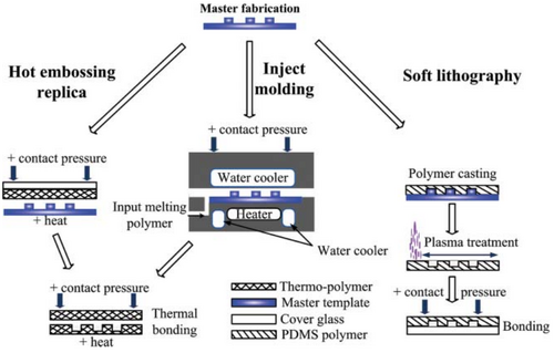
Hot embossing is a technique classified as a form of soft lithography or a variant of replica molding.1 Soft lithography is a technique which transfers a pattern onto an elastomer via a mold or stamp. Hot embossing uses pressure to precisely press the template into a heated polymer. This is an effective technique as the polymer used become amorphous or rubbery when exposed to elevated temperatures. Hot embossing is a technique commonly used due to its cost efficiency, high yield, and exactness. It has become a staple in commercial microfluidics. Currently, research is focusing on improving these molding technologies and potentially developing new processes in this pursuit.3
Process
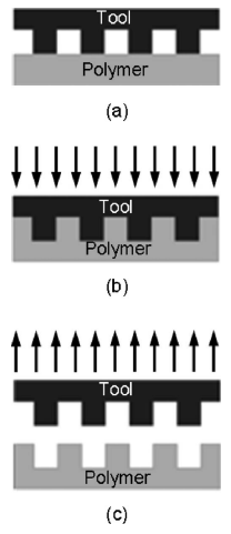
To create a microfluidic device with hot embossing, a thermosoftening plastic/polymer is placed between mold(s)/tools.2 Then, the tool and polymer are heated past the glass transition temperature of the plastic to make the plastic pliable. (Figure 2a). The patterned tool presses into the polymer so that the polymer fills in the gaps of the tool, effectively being embossed (Figure 2b). The polymer and tool are then allowed to cool below the glass transition temperature as to remove the tool as to obtain the resulting polymer device (Figure 2c).4
Factors that can impact the resulting plastic include the temperature of the heated materials, alignment of the tool, the duration of each step, and the pressure applied during the process.4
Materials
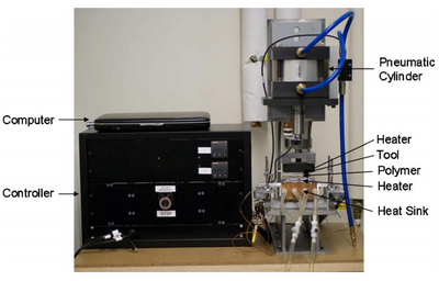
The thermoplastics most often used for hot embossing include: polycarbonate (PC), cyclic olefin copolymer (COC), and polymethylmethacrylate (PMMA).2 Materials often used for molds include nickel and silicon.5 Polymers can also be used as molds, as long as the Tg of the material is higher than the device's polymer.6 The metal mold is often created first in a glass or silicon wafer using photolithography. The silicon wafer is in the same pattern as the future polymer created. A metal like nickel is then layered onto the wafer and then electroplated.5 Other materials include pneumatic cylinders to evenly distribute constant pressure to emboss, heaters for both the tool and the polymer, and a heatsink for the the polymer to quickly cool the polymer. An experimental equipment set up is shown in Figure 3.
Advantages and Challenges
Advantages
Overall, hot embossing is a cost effective process, where a tool can be reused along with the other technology. The material consumed is the thermoplastic. It is relatively rapid and allows for precise devices to be made which makes hot embossing an excellent industrial process. Embossing can accomplish micro- and nanoscale aspects.7 The tools are relatively inexpensive and durable in comparison to injection molding.3 Because of the small distance that the thermoplastic moves (instead of being injected), the created device is less stressed and shrinks less.4 Aspect ratios (height/diameter) for micro hot embossing on average range from 0.1 to 10.8 For reference, a groove on a CD has an aspect ratio of 0.2.9 In some cases, aspect ratios of 25 to 40 have been achieved using microcasting, a type of hot embossing that uses metal alloy sheets and silicon templates.10
Challenges
Due to the higher temperatures of this process, the polymer material is restricted to the thermoplastic class. It can also prove to be relatively difficult to achieve three dimensional structures that are complicated as removal of the tool may destroy these features.3
Applications
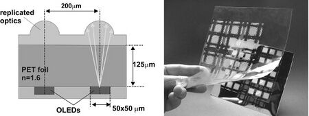
There are plenty of applications for hot embossing because of how cheap and reliable it is. Areas include optics, microelectromechanics (MEMs), and biomedical applications.8
Optics
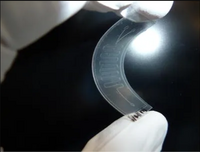
Within the area of optics, lenses for LED and OLEDs can be created using polycarbonate and films for photovolatic arrays can be made using PVC.8
MEMs
MEMs such as microreactors and flow pumps can be embossed using PMMA. Hot embossing has become popular in this field of research because of how environmentally friendly and cost effective it is in comparison to silicon.8
Biomedical
Hot embossing can produce biomedical devices like microfluidic chips for drug delivery or protein crystallization.5, 7 Other devices include micro needles or scaffolds used in tissue engineering, typically made from PMMA, PS or PDMS.8
References
1 Chen, Y. Application of nanoimprint lithography/hot embossing: a review Applied Physics A, 2015, 121, 451-465. [1]
2 Gale, B.K; Jafek, A.R; Lambert, C.J; Goenner, B.L; Moghimifam, H; Nze, U.C; Kamarapu, S.K. A Review of Current Methods in Microfluidic Device Fabrication and Future Commercialization Prospects Inventions, 2018, 3, 60, 1-25. [2]
3 Wu, J; Gu, M. Microfluidic sensing: state of the art fabrication and detection techniques Journal of Biomedical Optics, 2011, 16, 8, 1-12. [3]
4 Eusner, T; Hale, M; Hardt, D.E. Process Robustness of Hot Embossing Microfluidic Devices Journal of Manufacturing Science and Engineering, 2010. 16, 8. [4]
5 Goral, V.N; Hsieh, Y; Petzold, O.N; Faris, R.A; Yuen, P.O. Hot embossing of plastic microfluidic devices using poly(dimethylsiloxane) molds Journal of Micromechanics and Microengineering 2011 21. [5]
6 Guha, S; Perry, S.L; Pawate, A.S; Kenis, P.J.A. Fabrication of X-ray compatible microfluidic platforms for protein crystallization Sensors and Actuators, 2012, 174, 1-9. [6]
7 Jeon, J.S; Chung, S; Kamn, R.D; Charest, J. L. Hot embossing for fabrication of microfluidic 3D cell culture platform Biomedical Microdevices, 2011, 13, 2, 325-333. [7]
8 Peng, L; Deng, Y; Yi, P; Lai, X. Micro hot embossing of thermoplastic polymers: a review Journal of Micromechanics and Microengineering, 2014, 24. [8]
9 Becker, H; Heim, U. Hot embossing as a method for the fabrication of polymer high aspect ratio structures Sensors and Actuators, 2000, 83, 130-135. [9]
10 Romano, L; Vila-Comamala, J; Kagias, M; Vogelsang, K; Schift, H; Stampanoni, M; Jefimovs, K. High aspect ratio metal microcasting by hot embossing for X-ray fabrication Microelectric Engineering, 2017, 176, 6-10. [10]
11 Metwally, K; Robert, L; Queste, S; Gauthier-Manuel, B; Khan-Malek, C. Roll manufacturing of flexible microfluidic devices in thin PMMA and COC foils by embossing and lamination Microsystem Technologies, 2012, 18, 199-207. [11]
12 Gale, M. T; Gimkiewicz, C; Obi, S; Schnieper, M; Sochtig, J; Thiele, H; Westenhofer, S. Replication technology for optical microsystems Optics and Lasers in Engineering, 2005, 43, 373-386. [12]
