Wet Etching - Eric Ying
Wet Etching is a process in microfabrication, after lithography, where chemicals are used to remove layers of a wafer.[1] Wafers, also called substrates, are typically planar surfaces where thin layers of materials are added to serve as a foundation for electronic and microfluidic devices; the most common wafers are made of silicon or glass.[1] Wet etching is an important process in semiconductor manufacturing, micromachines, and microfluidic devices that require microscale features to either optimize performance or create laminar flow regimes that are near impossible to obtain on the macroscale.[1] It is commonly used for layered applications due to being able to easily control z axis etching by altering etchant concentration and etch time. Disadvantages include lots of chemical waste, many of which are highly acidic and multistep processes.[1]
Before etching, areas of substrate need to be masked off to get the detailed features needed for a device. In a process called photolithography, a light sensitive photoresist is spin coated onto a wafer. The wafer is then prebaked to get rid of excess solvent in the photoresist.[1] A mask with cutouts of the desired features is then placed on top of the photoresist and UV light is used to cure any exposed photoresist. The coated wafer can now be wet etched to engrave a desired pattern into the wafer.[1]
Isotropic Etching
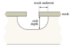
Isotropic etching, etching that is equal in all directions, is when a substrates orientation does not affect how an etchant removes material.[2] When the etchant, a corrosive chemical, is applied to a masked wafer, etching occurs in areas not covered by the mask in all directions at the same rate which creates rounded edges.[2] If the etchant is allowed to react long enough, the etchant will etch away substrate material under the mask called mask undercut as seen in Fig. 1. This can be avoided by washing off the etchant before it undercuts the mask, applying photoresist to the channel walls, then adding more etchant. The etchant rate can be easily controlled by adding a buffer to alter the concentration or by raising/lowering the temperature.[2]
Isotropic etching is not ideal when precise features need to be microfabricated due to the fact that it is not directionally specific and hard to control.[2]

Anisotropic Etching
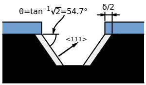
Anisotropic etching, etching that occurs at different rates in different directions, is depends on the orientation of the substrate’s crystalline planes.[3]
Due to silicon's single crystalline structure, some etchants are able to selectively etch silicon along certain planes or angles depending on the orientation of the silicon.[3] For example, using KOH as the etching chemical for silicon in the <100> crystal direction gives selectivity rates up to 400 times greater than using KOH to etch silicon in the <111> direction.[3] By altering time, etching chemical, and silicon crystal orientation, many different shapes and channels can be etched in the silicon wafer.[3]

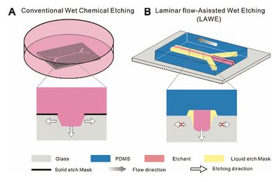
In order to anisotropically etch a non-crystal material such as glass, laminar flows of non-etching solutions need to be used to surround the etching chemical.[4] This creates a barrier between the substrate and the etchant and ensures only the desired areas in contact with the etchant will be removed.[4] ensures that only specific areas of the glass are being etched.[5]

Common Substrates and Etchants
| Substrate | Etchant | Rate |
|---|---|---|
| Aluminum | 19:1:1:2 H3PO4:HAc:HNO3:H2O
8:1:1 H3PO4:H2O2:H2O |
40 (Ang/s)
100 (Ang/s) |
| Chromium | Hydrochloric acid
1:1 HCl:Glycerine |
N/A
24 (Ang/s) |
| Gold | 3:1 Aqua regia HCl:HNO3 | 10-15 microns/min |
| Platinum | Aqua regia
Molten Sulfur |
|
| Silicon | 64:3:33 HNO3:NH4F:H20
61:11:28 Ethylenediamine:C6H4(OH)2:H2O |
100 (Ang/s)
78 (Ang/s) |
| Silicon Dioxide/Glass/Quartz | 3:2:60 HF:HNO3:H2O
NaCO3 @100°C |
2.5 (Ang/s)
296 (μm/h) |
| Titanium | Hydrofluoric acid
20% Sulfuric Acid |
N/A
1 (μm/min) |
References
- Mu, X.; Liang, Q.; Hu, P.; Ren, K.; Wang, Y.; Luo, G. Laminar Flow Used as “Liquid Etch Mask” in Wet Chemical Etching to Generate Glass Microstructures with an Improved Aspect Ratio. Lab on a Chip 2009, 9 (14), 1994–1996. doi:10.1039/b904769g
- Love, J. C.; Paul, K. E.; Whitesides, G. M. Fabrication of Nanometer-Scale Features by Controlled Isotropic Wet Chemical Etching. Advanced Materials 2001, 13 (8), 604–607. doi:10.1002/1521-4095(200104)13:8<604::AID-ADMA604>3.0.CO;2-J
- Bean, K. E. Anisotropic Etching of Silicon. IEEE Transactions on Electron Devices 1978, 25 (10), 1185–1193. doi:10.1109/T-ED.1978.19250
- Lee, D. B. Anisotropic Etching of Silicon. Journal of Applied Physics 1969, 40 (11), 4569–4574. doi:10.1063/1.1657233
- Bassous, E. Fabrication of Novel Three-Dimensional Microstructures by the Anisotropic Etching Of. IEEE Transactions on Electron Devices 1978, 25 (10), 1178–1185. doi:.1109/T-ED.1978.19249
- Wolf, S.; Tauber, R. N. Silicon Processing for the VLSI era; Lattice Press: Sunset Beach, CA, 1986. ISBN 0-9616721-3-7.
- Wet chemical etching of metals and semiconductors. https://cleanroom.byu.edu/wet_etch (accessed Feb 27, 2022).
