CHEM-ENG590E Wiki Textbook:Microcontact Printing: Difference between revisions
| Line 43: | Line 43: | ||
<gallery heights=200px widths=400px perrow="2"> | <gallery heights=200px widths=400px perrow="2"> | ||
Image: Fabricated nanocantilever array.png|'''Figure X.''' Salomon et al. fabrication an array of nanocantilevers on the scale of 10<sup>5</sup> nanocatilevers/cm<sup>2</sup>. | Image: Fabricated nanocantilever array.png|'''Figure X.''' Salomon et al. fabrication an array of nanocantilevers on the scale of 10<sup>5</sup> nanocatilevers/cm<sup>2</sup>. | ||
Image: IgGandBSAPrinting.png|'''Figure X.''' | Image: IgGandBSAPrinting.png|'''Figure X.''' Two methods of printing were used, resulting in both inked surfaces of BSA underneath the cantilevers and solely around the cantilevers. (1) Inking the stamp with IgG. (2) Washing and drying the stamp. (3) Cleaning outside the stamp grooves. (3B) Inking the stamp with BSA. (4) Printing after aligning the stamp and the chip. (4A) Incubating the chip with BSA. (5) Result. | ||
</gallery> | </gallery> | ||
</div> | </div> | ||
Revision as of 22:44, 14 April 2016
Microcontact Printing


Microcontact printing (MCP) is a technique of flow patterning that utilizes soft lithography to create a polydimethylsiloxane (PDMS) "stamp" in order to print micro-scale patterns. The concept of microcontact printing was first published in a 1993 paper written by George Whitesides and Amit Kumar of Harvard University. Their original goal was to use microcontact printing for micromachining. Since then, microcontact printing has been used for a variety of applications from biomaterial patterning to micro electronics.[2]
Procedure
Prepare Etched Silicon Master and PDMS Stamp
Using standard photolithography techniques, a silicon master must be created. A PDMS stamp can then be created with soft lithography. The silicon master can be reused to create multiple stamps, and each stamp can be used for multiple stampings
Ink Stamp and Apply Stamp to Substrate
The PDMS stamp is dipped into the "ink" of interest, and then applied to the substrate. Inking and stamping times vary depending on the properties of the ink and substrate.
Advantages
- Relatively cheap and simple process
- Minimal cleanroom time (only necessary to create the etched master)
- Multiple stamps can be created from a single etched master
- Reusable stamps
- Possibility to be scaled up and automate parts of the process
- Printing requires less “ink” than flow coating for patterning
- Can print on non-flat surfaces
Applications
Micromachining[2]
Microcontact printing originates with research in micromachining applications by Whitesides et al. The Whitesides Group demonstrated a novel form of microfabrication by printing self-assembled monolayers, or SAMs, of alkanethiol (a common 'ink') on a gold support (a common substrate). The ink then acted a form of photoresist in wet etching of the gold substrate by protecting the gold from corrosion caused by the etchants. Additional complex etching methods may be employed to further achieve high resolution microstructures. The true value of this method is that it avoids the repeated use of traditional photolithographic techniques in micromachining. They also demonstrated that microcrystal arrays were capable of being fabricated using their novel microcontact printing approach.
Biomaterial Patterning[5]

Cell-cell interactions may be studied using micropatterning techniques like printing. Bhatia et al. demonstrated microcontact printing allowed spatial control over liver cell populations, and thus allows a highly sophisticated method of investigation of cell growth, movement, shape, and death. In this study, collagen structures were immobilized under a patterned photoresist mask. The collagen then acted as an adhesive extracellular matrix for a patterning of hepatocytes and nonparenchymal cells. The heterotypic cell interactions in this microenvironment were then studied.
Biosensors[11]
Microcontact printing has also been employed in biosensor fabrication. Salomon et al. demonstrated precise printing of an antibody IgG and an antifouling compound BSA on a nanocantilever structure array. Cantilevers are a common structure used in biosensors, and an array of nanocantilevers allows for high selectivity and precise detection. The IgG was printed on the nanocantilevers, while the BSA was printed underneath and around the nanocantilevers.
-
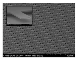 Figure X. Salomon et al. fabrication an array of nanocantilevers on the scale of 105 nanocatilevers/cm2.
 -
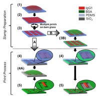 Figure X. Two methods of printing were used, resulting in both inked surfaces of BSA underneath the cantilevers and solely around the cantilevers. (1) Inking the stamp with IgG. (2) Washing and drying the stamp. (3) Cleaning outside the stamp grooves. (3B) Inking the stamp with BSA. (4) Printing after aligning the stamp and the chip. (4A) Incubating the chip with BSA. (5) Result.


Challenges of Microcontact Printing
- Stamp deformation
- Buckling
- Pairing
- Roof Collapse
- Contamination of substrate
- Stamp volume defects (shrinking or swelling)
- Ink mobility
Cutting Edge Techniques
Magnetic Field Printing[9]
High-Speed Printing[6]

Submerged Printing[7]
This technique attempts to address some of the stamp deformation issues by performing stamping within a non-compressible fluid. Bessueille et al. have shown that by stamping in a liquid, a much greater pressure can be applied to the stamp without deforming the pattern. additionally, higher aspect ratio features can be stamped. While conventional microcontact printing shows serious deformation over a ratio of 10:1, when submerged, a 46:1 ratio transfers perfectly, and ratios as high as 83:1 are still highly functional.
Liftoff Printing[8]
Liftoff printing is a technique that is intended to compensate for printing flaws caused by overly large aspect ratios. The technique was first used by Ricoult et al. to create an array of microdots which could not have been printed using conventional means. Instead of creating a stamp with an array of posts to print the dots, the team created a negative stamp, coated a flat piece of PDMS with their ink, and then lifted off the unwanted ink using the negative stamp. This left ink on the PDMS only in the micro dot array. This technique can be applied in similar situations where conventional stamping methods would fail.
Macro-Stamping[10]

Macro-Stamping is a technique developed by H. Lalo et al. which utilized a titration plate to create an array of micro dots of different ink. A stamp was created with an array of mili scale posts. The array was designed to be dipped into a titration plate and have each post go into a single well. The ends of the posts had micro scale dot arrays. By filling different wells in the plate with different ink, a macro array of micro arrays of different ink can be rapidly and repeatedly stamped.
References
1. Kaufmann, T.; Ravoo, B. J. Stamps, inks and substrates: polymers in microcontact printing. Polymer Chemistry. 2010, 1 (4), 371.
2. Wilbur, J. L.; Kumar, A.; Biebuyck, H. A.; Kim, E.; Whitesides, G. M. Microcontact printing of self-assembled monolayers: applications in microfabrication. Nanotechnology. 1996, 7 (4), 452–457.
3. Cau, J.; Lafforgue, L.; Nogues, M.; Lagraulet, A.; Paveau, V. Magnetic field assisted microcontact printing: A new concept of fully automated and calibrated process. Microelectronic Engineering. 2013, 110, 207–214. http://www.biosoftlab.com/index.php/biosoft-technologies/soft-lithography
4. Gross, G. W., et al. The use of neuronal networks on multielectrode arrays as biosensors. Biosensors and Bioelectronics. 1995, 70 (6-7), 553-567.
5. Bhatia, S.; Balis, U.; Yarmush, M.; Toner, M. Effect of cell-cell interactions in preservation of cellular phenotype: cocultivation of hepatocytes and nonparenchymal cells. Faseb Journal. 1999, 13 (14), 1883-1900.
6. Helmuth, J.; Schmid, H.; Stutz, R.; Stemmer, A.; Wolf, H. High-Speed Microcontact Printing. J. Am. Chem. Soc. 2006, 128 (29), 9296–9297.
7. Bessueille, F.; Pla-Roca, M.; Mills, C.; Martinez, E.; Samitier, J.; Errachid, A. Submerged Microcontact Printing (SμCP): An Unconventional Printing Technique of Thiols Using High Aspect Ratio, Elastomeric Stamps. Langmuir. 2005, 21 (26), 12060–12063.
8. Ricoult, S.; Pla-Roca, M.; Safavieh, R.; Lopez-Ayon, G.; Grütter, P.; Kennedy, T.; Juncker, D. Large Dynamic Range Digital Nanodot Gradients of Biomolecules Made by Low-Cost Nanocontact Printing for Cell Haptotaxis. Small. 2013, 9 (19), 3308–3313.
9. Cau, J.; Lafforgue L.; Nogues M.; Lagraulet, A.; Paveau, V. Magnetic field assisted microcontact printing: A new concept of fully automated and calibrated process. Microelectronic Engineering. 2013, 110, 207–214.
10. Lalo, H.; Cau, J.; Thibault, C.; Marsaud, N.; Severac, C.; Vieu, C. Microscale multiple biomolecules printing in one step using a PDMS macrostamp. Microelectronic Engineering. 2009, 86 (4–6), 1428–1430.
11. Salomon, S.; Leïchlé, T.; Dezest, D.; Seichepine, F.; Guillon, S.; Thibault, C.; Vieu, C.; Nicu, L.. Arrays of nanoelectromechanical biosensors functionalized by microcontact printing. Nanotechnology. 2012, 23 (49).
