Sandbox: Difference between revisions
No edit summary |
No edit summary |
||
| Line 3: | Line 3: | ||
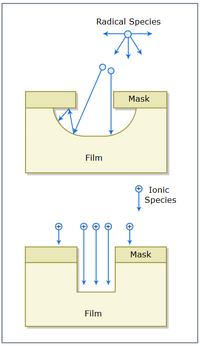
'''Dry etching''' (also known as plasma etching) is the process of removing material by exposing the material to an ion bombardment to form a pattern. Unlike many [https://openwetware.org/wiki/Wet_Etching_-_Eric_Ying wet etching] techniques, dry etching is an anisotropic process, allowing for etching of flat, lateral walls. Most dry etch techniques employ reactive ion etching (RIE) which combines physical etching with chemical etching to achieve a balance of selectivity and anisotropy. The process of dry etching is widely employed in the microfabrication of circuitboards by etching of silicon substrates as well as in the design of microfluidic devices. In recent years, dry etching has mostly replaced wet etching for fabrication of circuitboards. | '''Dry etching''' (also known as plasma etching) is the process of removing material by exposing the material to an ion bombardment to form a pattern. Unlike many [https://openwetware.org/wiki/Wet_Etching_-_Eric_Ying wet etching] techniques, dry etching is an anisotropic process, allowing for etching of flat, lateral walls. Most dry etch techniques employ reactive ion etching (RIE) which combines physical etching with chemical etching to achieve a balance of selectivity and anisotropy. The process of dry etching is widely employed in the microfabrication of circuitboards by etching of silicon substrates as well as in the design of microfluidic devices using materials such as polydimethylsiloxane (PDMS).<sup>[11]</sup> In recent years, dry etching has mostly replaced wet etching for fabrication of circuitboards. | ||
| Line 50: | Line 50: | ||
#Plasma etching with a microwave cavity plasma disk source. (1989). Vacuum, 39(10), 997. http://dx.doi.org/10.1016/0042-207x(89)90957-3 | #Plasma etching with a microwave cavity plasma disk source. (1989). Vacuum, 39(10), 997. http://dx.doi.org/10.1016/0042-207x(89)90957-3 | ||
#"Dry Etching.” MIT Courses: Electrical and Computer Science (6.152J/3.155J). MIT Open CourseWare. ocw.mit.edu/courses/electrical-engineering-and-computer-science/6-152j-micro-nano-processing-technology-fall-2005/lecture-notes/lecture17.pdf. | #"Dry Etching.” MIT Courses: Electrical and Computer Science (6.152J/3.155J). MIT Open CourseWare. ocw.mit.edu/courses/electrical-engineering-and-computer-science/6-152j-micro-nano-processing-technology-fall-2005/lecture-notes/lecture17.pdf. | ||
#Tanaka, Hiro, et al. “Onset of Wiggling in a Microscopic Patterned Structure Induced by Intrinsic Stress During the Dry Etching Process.” Journal of Applied Mechanics, vol. 81, no. 9, Oct. 2014, p. 091009., doi | #Tanaka, Hiro, et al. “Onset of Wiggling in a Microscopic Patterned Structure Induced by Intrinsic Stress During the Dry Etching Process.” Journal of Applied Mechanics, vol. 81, no. 9, Oct. 2014, p. 091009., http://dx.doi.org/10.1115/1.4027914. | ||
#Etching Processes, MEMSnet.org. Retrieved 12 April 2018, from www.memsnet.org/mems/processes/etch.html. | #Etching Processes, MEMSnet.org. Retrieved 12 April 2018, from www.memsnet.org/mems/processes/etch.html. | ||
#“BYU Cleanroom.” STS Multiplex ICP Etch | BYU Cleanroom, cleanroom.byu.edu/sts_icp. | #“BYU Cleanroom.” STS Multiplex ICP Etch | BYU Cleanroom, cleanroom.byu.edu/sts_icp. | ||
#Roozeboom, F., et al. “Cyclic Etch/Passivation-Deposition as an All-Spatial Concept toward High-Rate Room Temperature Atomic Layer Etching.” ECS Journal of Solid State Science and Technology, vol. 4, no. 6, July 2015, doi | #Roozeboom, F., et al. “Cyclic Etch/Passivation-Deposition as an All-Spatial Concept toward High-Rate Room Temperature Atomic Layer Etching.” ECS Journal of Solid State Science and Technology, vol. 4, no. 6, July 2015, http://dx.doi.org/10.1149/2.0111506jss. | ||
#Garra, J., et al. “Dry Etching of Polydimethylsiloxane for Microfluidic Systems.” Journal of Vacuum Science & Technology A: Vacuum, Surfaces, and Films, vol. 20, no. 3, 2002, pp. 975–982., http://dx.doi.org/10.1116/1.1460896. | |||
Revision as of 00:46, 13 April 2018

Dry etching (also known as plasma etching) is the process of removing material by exposing the material to an ion bombardment to form a pattern. Unlike many wet etching techniques, dry etching is an anisotropic process, allowing for etching of flat, lateral walls. Most dry etch techniques employ reactive ion etching (RIE) which combines physical etching with chemical etching to achieve a balance of selectivity and anisotropy. The process of dry etching is widely employed in the microfabrication of circuitboards by etching of silicon substrates as well as in the design of microfluidic devices using materials such as polydimethylsiloxane (PDMS).[11] In recent years, dry etching has mostly replaced wet etching for fabrication of circuitboards.
Mechanism
Dry etching is mostly driven by reaction of chemicals in plasma state. The plasma increases reactivity of chemicals, etching via a physical and chemical basis. Physical etching occurs from the bombardment of neutral particles while the chemical etching occurs from charged ions. A silicon substrate coated with an etching mask, with the etching mask leaving free the regions of the silicon substrate that are intended to be anisotropically etched, is subjected to an initial etching step. For this purpose a gas mix containing reactive species like SF6 or nonreactive noble gases such as Ar can be used. The composition of gas used will affect the selectivity for substrate and the degree of anisotropy of the process.[6] For example, since Ar is nonreactive, the majority of species will bombard the exposed areas, typically knocking off surface particles via nonselective momentum transfer when the ions have greater collision energy than the surface binding energy of the solid, removing and vaporizing the solid particles in a process known as sputtering. During the etching step, chemical reactive species and ions are generated in the reaction chamber aided by an electrical discharge of ionic species in the plasma.

Plasma Generation
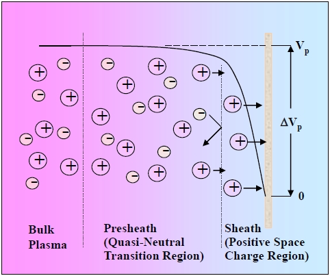
To perform dry etching the plasma must be generated first. The plasma is formed when electrons are accelerated to high energy states typically performed in high energy electric or magnetic fields using microwaves but more recently radiowaves. The plasma contains positive ions, electrons, reactive chemical species, and neutral particles all contained in one bulk state. Without a plasma, all the processes involved in etching require higher temperature. There are different ways to change the plasma chemistry and get different kinds of plasma etching or plasma depositions. One popular technique is to use an oscillating(AC) radio frequency wave to strip electrons from the gaseous species.[5] The field accelerates electrons, giving them a high velocity to escape the gas molecules and create ionic species, forming the plasma. Using an oscillating field allows the electrons to accelerate back and forth between electrodes, gaining momentum and charging the wafer surface. The ions are then attracted to the negatively charged surface, bombarding and neutralizing the surface. The process then repeats in a cycle. Plasma etchers implement a form of plasma confinement to concentrate plasma into a region of the apparatus to allow control of etch rates and feature distribution. There are many parameters such as pressure, gas composition, gas flowrates, and supply power which can be adjusted to give desired etching properties.[2] The plasma is confined by manipulating the properties of Debye sheaths which are transition layers between the plasma and solid. The Debye region is a result of the equilibrium formed from electrons bombarding the solid surface due to the higher electron temperature in comparison to plasma temperature, negatively charging it relative to the positive bulk plasma. This is tunable by adjusting the electric or magnetic field applied across the electrode.

Parallel Plate Etching
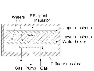
Parallel plate etching refers to the apparatus used in RIE. This mode of etching uses an electric field to generate the plasma, typically employing a small electrode to focus ions in a concentrated vertical direction to give a more anisotropic etch. The smaller the electrode area the greater the bias. By increasing the applied field strength, a greater degree of anisotropy can be achieved with deeper etches.[8]

Inductively Coupled Plasma Etching
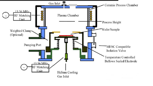
Inductively coupled plasma etching is a mode of etching in which an electromagnet is employed to generate a magnetic field for plasma production. This process doesn't require electrodes inside the chamber, thus reducing potential contamination. High plasma density can be achieved using lower pressures with this method, which allows a greater anisotropic etch to be achieved although greater damage to the mask and substrate can occur.[6]

Bosch Process
The Bosch process also known as deep reactive ion etching (DRIE) is a technique used to create high aspect ratio structures in silicon, allowing for very deep etches. It is able to etch defined features such as trenches, combs, and tongues anisotropically with a fair degree of selectivity in silicon substrate. The performance of this process, when done with microwave excitation (propagation ion etching) does not produce significant wall roughness. The Bosch process is widely used for obtaining relatively smooth sidewalls required for industrial applications in electronics and circuit boards. The process involves successive etching and deposition cycles to coat the sidewalls as etching progresses. Each cycle involves a typical ion bombardment and is followed with a deposition step of a chemically inert passivation layer (usually C4F8) on the newly exposed sidewalls, protecting them from reacting with chemical species, however there is a possibility of sputtering the layer on the sides although the majority of species bombard vertically on the bottom layer.[10] Without the passivation layer on the sidewalls the ions would react with substrate as deeper etches are made, leaving undesirable isotropic etch patterns. However, due to the nature of the technique, repeated cycles do result in small undulations in side walls due to small isotropic steps occurring between cycles. The process has been applied to the manufacture of flexible circuit boards, however deeper trenches for stretchable electronics required a titanium/gold bilayer hard mask.

Applications
Dry etching is useful for materials and semiconductors that are chemically resistant and are not able to be wet etched. When used with photolithography, silicon dioxide can be applied or removed to trace paths for circuits for application in electronics. Dry etching is used in conjunction with photolithographic techniques to shape certain areas of a semiconductor surface to form wells in material for electrical contacts or circuit channels or to otherwise remove portions of semiconductor layers where vertical sides are desired. The process also sees use in fabricating lateral high aspect ratio walls for microfluidic device channels.
References
- Plasma Potential & Sheath. (2018). Egloos.zum.com. Retrieved 24 February 2018, from http://egloos.zum.com/jinhwanlee/v/10888947
- Method of anisotropically etching silicon - Robert Bosch GmbH. (2018). Freepatentsonline.com. Retrieved 24 February 2018, from http://www.freepatentsonline.com/5501893.html
- Ghoneim, M., & Hussain, M. (2017). Flexible Electronics: Highly Manufacturable Deep (Sub-Millimeter) Etching Enabled High Aspect Ratio Complex Geometry Lego-Like Silicon Electronics (Small 16/2017). Small, 13(16). http://dx.doi.org/10.1002/smll.201770089
- Rawat. (2018). Etching. Slideshare.net. Retrieved 24 February 2018, from https://www.slideshare.net/deepak10rawat/etching-55985755
- Plasma etching with a microwave cavity plasma disk source. (1989). Vacuum, 39(10), 997. http://dx.doi.org/10.1016/0042-207x(89)90957-3
- "Dry Etching.” MIT Courses: Electrical and Computer Science (6.152J/3.155J). MIT Open CourseWare. ocw.mit.edu/courses/electrical-engineering-and-computer-science/6-152j-micro-nano-processing-technology-fall-2005/lecture-notes/lecture17.pdf.
- Tanaka, Hiro, et al. “Onset of Wiggling in a Microscopic Patterned Structure Induced by Intrinsic Stress During the Dry Etching Process.” Journal of Applied Mechanics, vol. 81, no. 9, Oct. 2014, p. 091009., http://dx.doi.org/10.1115/1.4027914.
- Etching Processes, MEMSnet.org. Retrieved 12 April 2018, from www.memsnet.org/mems/processes/etch.html.
- “BYU Cleanroom.” STS Multiplex ICP Etch | BYU Cleanroom, cleanroom.byu.edu/sts_icp.
- Roozeboom, F., et al. “Cyclic Etch/Passivation-Deposition as an All-Spatial Concept toward High-Rate Room Temperature Atomic Layer Etching.” ECS Journal of Solid State Science and Technology, vol. 4, no. 6, July 2015, http://dx.doi.org/10.1149/2.0111506jss.
- Garra, J., et al. “Dry Etching of Polydimethylsiloxane for Microfluidic Systems.” Journal of Vacuum Science & Technology A: Vacuum, Surfaces, and Films, vol. 20, no. 3, 2002, pp. 975–982., http://dx.doi.org/10.1116/1.1460896.
