Microtransfer Molding - Marissa Burgess, Ruptanu Banerjee, Vaishali Malik
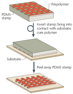
Microtransfer molding (μTM) is a form of soft lithography - a set of pattern transfer techniques that employs a patterned elastomer as a stamp, mask, or mold. The method of microtransfer molding is known for its applications in fabricating three dimensional structures on a microscale level and is popular for its use in the microfabrication of microelectromechanical systems (MEMS) devices. With the ever-increasing desire to miniaturize scientific and technological devices, techniques such as microtransfer molding along with other soft lithography techniques have gained more attention. Consumer products, biomedical instrumentation, and scientific devices are all potential applications of microtransfer molding. Microfluidic devices have become increasingly popular and are one of the most prominent areas of application for soft lithography techniques like microtransfer molding. The ability to produce three dimensional microfluidic systems would allow the creation of many new types of devices and permits to make existing devices more compact. Recent years have shown a growing interest in fabricating microstructures in a number of different applications including polymer-based integrated optical circuits, artificial bones, integrated microfluidic systems, photonic crystals, and catalytic reactors.[1]
Process of Microtransfer Molding
The process of microtransfer molding is illustrated in Figure 1. Briefly, in microtransfer molding, a polydimethylsiloxane (PDMS)-based mold called a "stamp" is utilized. The PDMS stamp contains recessed regions, or microchannels, that are manually filled with prepolymer or ceramic precursor. The PDMS stamp, filled with liquid prepolymer, is then inverted, and brought into contact with the substrate. Next, the polymer is cured, and the PDMS stamp is peeled away. This results in polymer microstructures on the substrate with a feature size as small as 1 µm, arranged based on the design of the channels in the PDMS stamp. This technique is a powerful tool for fabricating microfluidic devices with high precision, reproducibility, and versatility, making it an attractive option for researchers and manufacturers in a variety of fields. [2]
When fabricating microfluidic devices, the material used for microtransfer molding depends on their application and requirements. Nevertheless, there are a number of materials commonly used in microfluidics for microtransfer molding, including the following: PDMS, polyurethane (PU), poly(methyl methacrylate) (PMMA), epoxy resins, poly(ethylene terephthalate) (PET) and more. PDMS is widely used material for microfluidic devices due to its high optical clarity, biocompatibility, and ease of molding. Moreover, it can be used to build complex structures due to its flexibility. PDMS generally comes in two components including the prepolymer and the curing agent. The hardening of PDMS is achieved through the cross-linking of its polymer chains via thermal curing. Microstructures of both ceramic precursors and polymers (ZrO2, spin on glass) have successfully been made on a range of substrates including glass, Ag, Au, Si, and Si/SiO2. [2]
Advances in Microtransfer Molding
Two-polymer Microtransfer Molding
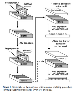
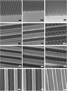
In two-polymer microtransfer molding (2P-µTM) is a variation of microtransfer molding that uses two different UV-curable prepolymers as both a filler and an adhesive for creation of microstructures with multiple layers of different polymers (Figure 2). The process is divided into five major steps: preparation of the mold, preparation of the stamp, transfer of first polymer layer, preparation and transfer of second polymer layer, finally the curing and release of microfluidic device. First a silicone or similar material mold is microfabricated with the desired microstructures, such as channels, chambers, or valves. Then the stamp is prepared by coating a thin layer of release agent, such as fluorinated silane, to facilitate the release of the transferred polymers. The stamp is then coated with a layer of polymeric material, such as PDMS, which is used to transfer the first polymer layer onto the substrate. A filling method called "wet-and-drag" (WAD) is employed - one drop of the first prepolymer is placed outside of a patterned section on a PDMS mold. Using a metal blade, the drop is dragged at a constant speed, controlled by mechanical actuators. Dragging the first prepolymer through the patterned area results in the polymer only filing the channels, without any residue. The stamp is then placed onto the mold and pressed against it to transfer the first polymer layer onto the stamp. The stamp is then peeled off the mold, leaving the first polymer layer on the stamp. The stamp is then aligned with the substrate and pressed against it to transfer the first polymer layer onto the substrate. A second stamp is then prepared by performing the WAD method a second time, which is coated with a different polymeric material, such as polystyrene (PS), that will be used to transfer the second polymer layer onto the substrate. The second stamp is aligned with the substrate and pressed against it to transfer the second polymer layer onto the first polymer layer. The substrate with the two polymer layers is then cured, typically by heating it to a specific temperature or UV exposure for a specified amount of time, to allow the polymers to crosslink and adhere to each other. Finally, the stamp is peeled off the substrate, leaving the two-polymer microstructure on the substrate. By using a substrate with a pre-stacked structure, a structure with any number of layers can be created. [3] [4]
Several advantages can be noted to using two-polymer microtransfer molding techniques over traditional microtransfer molding methods. Microstructures created with two-polymer microtransfer molding allows for controlled mechanical properties which are important for applications in microfluidics and microelectromechanical systems. Using more than one polymer for microtransfer, allows for creation of structures with different optical properties. Different refractive indices or light scattering properties allow for applications in optical sensing and imaging. Furthermore, biocompatible polymers can be used to create microstructures with biological functionality with the ability to selectively bind to specific biological molecules. For example, one polymer material can be functionalized with biomolecules, such as antibodies that selectively bind to specific target molecule. The second polymer can then be used to create a microstructure that selectively captures the target molecule, allowing for the creation of biosensors and diagnostic devices. [4]
Pin Printing Microtransfer Molding
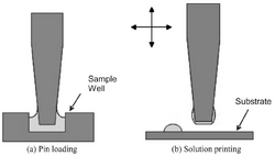
Pin printing microtransfer molding (PP-µTM) is a variation of microtransfer molding that allows for the creation of high-density arrays of microstructures. The preparation of the mold and the stamp is similar as previously described but the loading of the stamp is different from the traditional microtransfer molding technique. Here, a method called solid pin contact printing is used; where a solid pin is loaded with the material to be transferred, typically by dipping it into a solution or by using a pipette to apply the material directly to the pins (Figure 3). The stamp is aligned with the mold and pressed against it to transfer small volumes of the material onto the mold. The stamp is then peeled off the mold, leaving small droplets of the material on the mold, which correspond to the microstructures. The mold is then aligned with the substrate and pressed against it to transfer the microstructures onto the substrate. The microstructures are typically transferred in an array format, allowing for the creation of high-density arrays of microstructures. [5]
This method allows for the creation of high-density arrays of microstructures, which is useful for applications that require a large number of microstructures in a small area. The microstructures are highly precise, with dimensions as small as a few microns. This is a relatively fast process, allowing for the creation of thousands of microstructures in a matter of minutes. Although the solid pin printing method is relatively straightforward, creating solid pins is a complex process. Typically, pins are made from metals like stainless steel, tungsten, and titanium, which pose challenges in terms of manufacturing. Conventional mechanical machining techniques have limitations and can cause the pins to undergo stresses that may result in corrosion and deformation. [5]
Electrically Modulated Microtransfer Molding
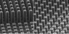
Electrically modulated microtransfer molding (EMµTM) is a variation of microtransfer molding that uses an electric field to manipulate the transfer of the patterned polymer layer. This technique offers more precise control over the transfer process and can be used to create complex structures with high aspect ratios and intricate geometries. The EMµTM process begins by preparing a substrate with a patterned electrode layer. A thin layer of a sacrificial material, such as a photoresist, is then spin-coated onto the substrate. This sacrificial layer is used to create a mold for the polymer layer. A layer of a conductive polymer is then spin-coated on top of the sacrificial layer, followed by a layer of the desired non-conductive polymer. The conductive polymer layer serves as an electrode, and an electric field is applied to the substrate to modulate the transfer of the non-conductive polymer layer. When the electric field is applied, the conductive polymer layer becomes charged, and this charge induces an electrostatic force on the non-conductive polymer layer. The force causes the non-conductive polymer layer to adhere to the mold created by the sacrificial layer. After the transfer process is complete, the sacrificial layer is removed, leaving behind the patterned non-conductive polymer layer on the substrate. The electric field can be adjusted during the transfer process to control the thickness and pattern of the transferred polymer layer (Figure 4). [6 ]
EMµTM offers several advantages over traditional microtransfer molding techniques. It enables the creation of complex patterns and high aspect ratio structures, and it allows for precise control over the thickness and shape of the transferred polymer layer. Additionally, the use of an electric field provides a non-contact transfer process, reducing the risk of damage to delicate structures. The ability to create electrically modulated micropillar arrays over a large area has opened up new frontiers in surface engineering, biotechnology, and microfluidics.[6 ]
Advantages and Challenges
Advantages
Several significant benefits can be noted regarding the process of microtransfer molding. The entire process is rapid, with the capability of replicating microstructures in five minutes or less. Both isolated and interconnected structures can be generated as well. Using microtransfer molding, structures composed of two materials (for example, polymer doped with dye) can also be produced with a uniform concentration of the dopant over the entire pattern. Other techniques such as microfluidic mold insert casting (MIMIC) often produce a concentration gradient in the components because one component may be adsorbed by the PDMS master while prepolymer is filling the channels. In this technique, a mold insert is fabricated with a desired microfluidic pattern, and is then placed into a larger mold. The larger mold is then filled with a liquid polymer, which is cured to create a solid replica of the mold insert. The mold insert is then removed, leaving behind a microfluidic structure that matches the original pattern of the mold insert. MIMIC allows for the creation of more complex microfluidic structures than traditional microtransfer molding, and can be used to create devices with multiple layers or channels. [11] Microtransfer molding is also much less sensitive to changes in prepolymer viscosity over time during the process due to how fast the process is. Another advantage of microtransfer molding is that it can be applied to a broad range of materials. Many different structures can be replicated by the microtransfer molding process due to the PDMS mold’s elastic nature. Structures with large overhangs [8] (up to 20 µm) and high aspect ratios [9] (as high as 15:1) can be fabricated. Most significantly, in contrast to other patterning techniques, microtransfer molding can form structures on contoured surfaces in addition to flat surfaces (Figure 5). [7] This trait is necessary for the microfabrication of 3-D structures, as the polymer can be deposited and cured layer by layer into the desired 3-D shape. Microtransfer molding also has low capital and operating costs, and it is cheap to create which results in the ability to rapidly prototype. [4]
Challenges
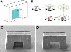
Stamp or mold deformation is one of the main challenges that can be encountered during microtransfer molding. For example, the precursors used to create ceramics are generally liquid-based sol or colloidal suspensions, largely consisting of organic and aqueous material that must be removed when the liquid is converted into a solid. During the drying and sintering process, the thin film may diverge from the original shape from shrinking. For similar reasons, closed loop structures cannot be replicated by microtransfer molding in one single step. This is because as the elastomeric resin pours over the loop and is cured, the loop ends up becoming topologically locked in the elastomer, unable to be released (Figure 6). [8 ] Layer by layer fabrication approaches are thus necessary to mold closed loops via microtransfer molding.
Applications
Microtransfer molding holds great promise in the design of microfluidic devices. An example is the development of a chip for capillary electrophoresis separation.[12] The advantage of such system is that they are user directed and inexpensive to make. It is possible for anyone to produce microfluidic devices at a large scale by using this replica molding technique in a very short time.
µTM has been used to deposit polymers to achieve nanostructured patterns.[13] This work demonstrated that µTM can be used to deposit multilayer patterns of G4 aldehyde dendrimers (CHO end group) with a nanometer scale resolution and the patterned structures are stable over long periods of time. These dendrimer nanostructures thus can be used for studying proteins by conjugating the CHO end group the amine group on the proteins.
µTM is also being employed along with electrophoretic deposition [14]. µTM is used here to create a PDMS stamp which is then used to pattern an organic soluble ink on indium tin oxide. Gold nanoparticles in colloidal form was then deposited by electrophoretic deposition with an anodic bias between the colloidal solution and indium tin oxide base.
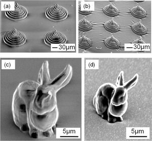
A two-photon microfabrication technique is being used along with µTM to fabricate 3-D carbon microstructures. [11] This was achieved by developing a new type of polymer that is suitable for carbonization via pyrolysis. 3-D PDMS mold was designed using µTM and the polymer was injected into the mold followed by UV curing and carbonization. The 3-D structures produced by this technique yielded in high resolution patterned 3-D structures (Figure 7).
References
- Van Assenbergh, P.; Meinders, E.; Geraedts, J.; Dodou, D. Nanostructure and Microstructure Fabrication: From Desired Properties to Suitable Processes. Small 2018, 14 (20). https://doi.org/10.1002/SMLL.201703401.
- Weibel, D. B.; DiLuzio, W. R.; Whitesides, G. M. Microfabrication Meets Microbiology. Nat. Rev. Microbiol. 2007 53 2007, 5 (3), 209–218. https://doi.org/10.1038/nrmicro1616.
- Zhao, X.; Xia, Y.; Whitesides G. Fabrication of Three-Dimensional Micro-Structures: Microtransfer Molding. Advanced Materials Communications 1996, 8, (10) https://doi.org/10.1002/adma.19960081016.
- Lee, J. H.; Kim, C. H.; Ho, K. M.; Constant, K. Two-Polymer Microtransfer Molding for Highly Layered Microstructures. Adv. Mater. 2005, 17 (20), 2481–2485. https://doi.org/10.1002/ADMA.200500721.
- Barbulovic-Nad, I.; Lucente, M.; Sun, Y.; Zhang, M.; Wheeler, A.; Bussmann, M. Bio-Microarray Fabrication Techniques—A Review, Critical Reviews in Biotechnology, (2006) 26:4, 237-259, https://doi.org/10.1080/07388550600978358.
- Li, X.; Tian, H.; Shao, J.; Ding, Y.; Liu, H. Electrically Modulated Microtransfer Molding for Fabrication of Micropillar Arrays with Spatially Varying Heights. Langmuir 2013, 29 (5), 1351–1355. https://doi.org/https://doi.org/10.1021/la304986e.
- Senn, T.; Esquivel, J. P.; Lörgen, M.; Sabaté, N.; Löchel, B. Replica Molding for Multilevel Micro-/Nanostructure Replication. J. Micromechanics Microengineering 2010, 20 (11), 115012. https://doi.org/10.1088/0960-1317/20/11/115012.
- LaFratta, C. N.; Baldacchini, T.; Farrer, R. A.; Fourkas, J. T.; Teich, M. C.; Saleh, B. E. A.; Naughton, M. J. Replication of Two-Photon-Polymerized Structures with Extremely High Aspect Ratios and Large Overhangs. J. Phys. Chem. B 2004, 108 (31), 11256–11258. https://doi.org/https://doi.org/10.1021/jp048525r.
- Kim, K.; Park, S.; Lee, J. B.; Manohara, H.; Desta, Y.; Murphy, M.; Ahn, C. H. Rapid Replication of Polymeric and Metallic High Aspect Ratio Microstructures Using PDMS and LIGA Technology. Microsyst. Technol. 2002 91 2002, 9 (1), 5–10. https://doi.org/10.1007/S00542-002-0194-6.
- LaFratta, C. M.; Li, L.; Fourkas, J. T. Soft-Lithographic Replication of 3D Microstructures with Closed Loops. Proc. Natl. Acad. Sci. U. S. A. 2006, 103 (23), 8589–8594. https://doi.org/https://doi.org/10.1073/pnas.0603247103.
- Daicho, Y.; Murakami, T.; Hagiwara, T.; Maruo, S.; Wang, C.; Zaouk, R.; Park, B. Y.; Madou, M. J. Formation of Three-Dimensional Carbon Microstructures via Two-Photon Microfabrication and Microtransfer Molding. Opt. Mater. Express, Vol. 3, Issue 6, pp. 875-883 2013, 3 (6), 875–883. https://doi.org/10.1364/OME.3.000875.
- Duffy, D. C.; McDonald, J. C.; Schueller, O. J. A.; Whitesides, G. M. Rapid Prototyping of Microfluidic Systems in Poly(Dimethylsiloxane). Anal. Chem. 1998, 70 (23), 4974–4984. https://doi.org/10.1021/AC980656Z.
- Thibault, C.; Severac, C.; Trévisiol, E.; Vieu, C. Microtransfer Molding of Hydrophobic Dendrimer. Microelectron. Eng. 2006, 83 (4–9), 1513–1516. https://doi.org/10.1016/J.MEE.2006.01.213.
- Bailey, R. C.; Stevenson, K. J.; Hupp, J. T. Assembly of Micropatterned Colloidal Gold Thin Films via Microtransfer Molding and Electrophoretic Deposition. Adv. Mater. 2000, 12 (24), 1930–1934. https://doi.org/10.1002/1521-4095(200012)12:24%3c1930::AID-ADMA1930%3e3.0.CO;2-F.
- Chang, C.; Yang, S.; Huang, L.; Jeng, T. A novel method for rapid fabrication of microlens array using micro-transfer molding with soft mold. Journal of Micromechanics and Microengineering. (2006) 16 (5) https://doi.org/10.1088/0960-1317/16/5/017.
- Cell Kit Ying, W.; O.C.T, C.; Bing, X.; Matthew Ming Fai, Y. Using PDMS microtransfer molding (µTM) for polymer flip chip. IEEE - 53rd Electronic Components and Technology Conference, (2003) pp. 652-657, https://doi.org/10.1109/ECTC.2003.1216351.
- Zhao, X.; Xia, Y.; Whitesides G. Soft lithographic methods for nano-fabrication. J. Mater. Chem. (1997) 7, 1069-1074 https://doi.org/10.1039/A700145B.
