Microfluidic Sensing- Nanomaterials based- Xiaoyu Zhang
Nanomaterials
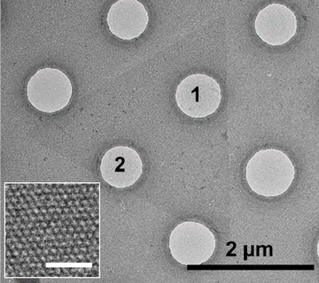
A nanomaterial is a material with any external dimension in the nanoscale (size range from approximately 1 – 100 nm) or having internal structure or surface structure in the nanoscale.1 Figure 1,2 show the electron micrograph and optical image of MoS2 and graphene, which are typical nanomaterials. When materials are scaled down to nanoscale, the great promotion of surface to volume ratio along with the appearance of quantum effects lead to a significant improvement of material characteristics, which make nanomaterials are promising for replacing macroscale materials in many areas like life science. What is more, the scalability also broadens the application fields of nanomaterials.
In the past years, nanomaterials (e.g. graphene, carbon nanotubes, MoS2, WSe2) have exhibited attractive characteristics, such as high detection sensitivity, good compatibility with planar nanofabrication processes, high surface to volume ratios and excellent scalability, which are different from those materials have at macroscopic level and makes nanomaterials highly sensitive to changes of surface chemistry, thus enabling nano-sensors to achieve extremely low limit of detection (LOD).2-5 Combined with microfluidics, nanomaterial-based microfluidic sensor paves a way to overcome some immediate challenges like precise bio-detection and ultralow velocity monitoring in the sensing area, the specific works will be introduced in the following parts.

Biomolecule Quantification
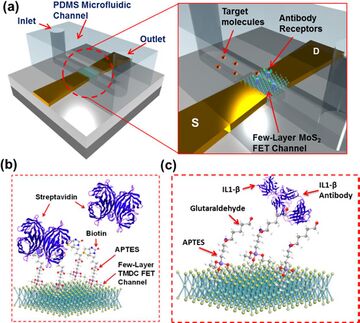
Figure 3 illustrates the MoS2-based field effect transistor (FET) biosensor, which is integrated with a polydimethylsiloxane (PDMS)-based microfluidic channel to quantification the different kinds of biomolecules such as fM-level biomarkers (different molecules can be testd with the change of detection receptors) in input solution. In the device, MoS2 acts as local gate of the FET. When the concentration of target molecules change, the induced electromotive force from molecules to MoS2 also change, which alter the local gate voltage, thus the concentration change of molecules can lead to the shift of the transistor I-V curve. The combination of MoS2 and microfluidic channels solves the challenges associated with the poor compatibility between electronic structure and liquid analytes in traditional sensors and provides rapid, low-noise, high specific biomolecule quantification at femtomolar levels.
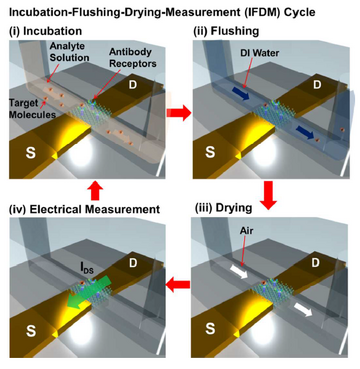
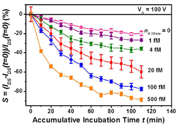
The running processes of the device can be divide into four steps as figure 4 shows: incubation, flushing, drying, and electrical measurement. The target molecules solution is infused into the channel and bind with the receptors in the incubation stage, DI water flushing is followed to remove the molecules not bind with receptors in the previous stage. Drying by dry air is the third step to remove water, thus the ion screening which forms at the interface between fluid and nanomaterials can be avoided. Electrical measurement is the last step to measure the I-V curve of the FET. After running multiple cycles of the whole 4 steps continually, the relationship between the response signal and time can be built and the concentration of molecules can be derived based on the difference of current drop rate of various concentrations.(figure 5) The multiple cycles test is able to avoid the influence of electrochemical damage caused by liquid-solution, nonspecific adsorption of molecules to the sensor and ion screening, which enhance the sensitivity, specificity, signal-to-noise ratio (SNR) and durability of the device.3
Environmental sensing
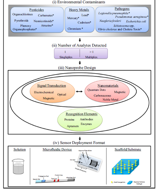
Nanomaterial based microfluidic sensors can also be used for environmental sensing to monitor and characterize the change of environments such as temperature, pressure and chemical components. Figure 6 shows a general process flow of nano-sensor design for environmental contaminants detection and can be used as a guide for real application. In general, the nano-sensors includes three different components. First, the nanomaterial is needed to interact with target chemicals while a specificity element is also needed for recognition. What is more, an effective method to transduce the signal which provides the information of the presence of the target analyte is also important. Such divisions actually can be used to characterize every nanosensor.5
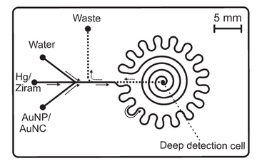
An example of a nanomaterial-based microfluidic sensor for heavy metals and pesticide detection is followed to give more details about this area. As Figure 7 shown, heavy metals and pesticides (two important environmental contaminants) are detected by a gold nanoparticle-based microfluidic sensor with the characteristics of rapid and in-filed detection. The size-dependent colorimetric and fluorescent properties of the gold nanoparticles overcome the shortcoming that low or even no fluorescence of most environmental samples, the presence and concentration of target contaminants can be easily recognized by optical detection methods after the mix of nanoparticles and contaminants. In this work, the limit of detection of 0.6 mg/L and 16 mg/L is demonstrated for heavy metal mercury and dithiocarbamate pesticide ziram, respectively. The result showed that the combination of the gold nanoparticles with excellent optical properties and microfluidic chips is promising to build simple, portable and sensitive sensors for the detection of environmental contaminants.8
Flow sensing
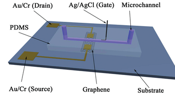
Nanomaterial based microfluidic sensors can also be used for flow velocity detection. Figure 8 illustrates the structure of a solution-gated graphene field transistors (SGGT) flow meter which integrated with a microfluidic system. When fluid is infused into the microchannel, the pressure gradient of fluid inside the microchannel leads to the movement of the electrical double layer (EDL) at the interface of fluid and graphene, and the streaming potential formed because of the potential difference between two ends of the channel. The streaming potential changes when adjusting the velocity and the output of transistor change simultaneously. Based on measuring the streaming potentials in microfluidic channels, the relationship between the response curve of the SGGT and the flow velocity can be built, which indicates that the SGGT is a promising transducer for measuring flow velocity in microchip.9
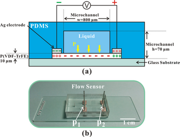
Besides graphene, aligned piezoelectric ploy nanofiber also shows the potential to be used for flow detection in a microfluidic environment (Figure 9). The fluid is infused into the microchannel and flow through the nanofibers, the potential of the nanofibers change with the change of flow velocity due to the piezoelectricity of the material. The voltage can then be converted to the velocity of fluid calibrated by the pre-established voltage-velocity relationship. By the use of this method, the flow rates ranging from 13 µl/h to 301 µl/h with a sensitivity of 0.36 mV per 1 µl/h is demonstrated.10 This work is an excellent example of combining the advantages of the large specific area and high sensitivity nanomaterials with microfluidic techniques, which can control and manipulate fluid efficiently.
Ion screening
While the nanomaterial-based microfluidic sensors have shown excellent spatial resolution and sensitivity and are promising for applications in areas of bio-sensing, environmental sensing, chemical sensing and so on. Most of these sensors have been limited to be used in the solution with relatively low ionic strength because of the existence of ion screening.11-13 To be more specific, in an ionic solution, a charged surface attracts counterions from the solution, forming an electrical double layer (EDL), which effectively screening off the charges and the nanomaterials cannot receive the signal from the solution.
The video illustrates the forming process of the electrical double layer (EDL).14
In order to overcome the challenge of ion screening, some techniques have been proposed. There are two main ways that the ion screening can be overcome, one is adding materials at the interface between fluid and nanomaterial and another one is playing with an external electrical signal.
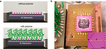
For the first way, a porous and biomolecule permeable polymer layer is added on the surface of the nanomaterial as shown in Figure 10, the polymer layer dramatically changes the dielectric properties in aqueous solutions, thus reducing the impact of screening and making it possible to detect analytes directly in real-time in physiology-relevant high ionic strength solutions.15
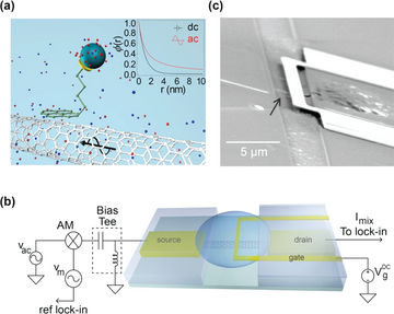
High frequency can also be used to detect beyond the ion screening that happened at the interface between nanomaterial and solution. Figure 11 shows a high-frequency single-walled carbon nanotube (SWNT) FET sensor. The high-frequency input signal alternates the molecular dipole field inside the solution, which successfully decreases the influence of ion screening. The detection of 100 mM buffer solution is achieved in the research.16
References
1. ISO, ISO/TS 80004-1:2015. Nanotechnologies—vocabulary—part 1: core terms. Geneva: International Organization for Standardization; 2015. https://www.iso.org/obp/ui/#iso:std:iso:ts:80004:-1:ed-2:v1:en
2. Holzinger, M., Le Goff, A., & Cosnier, S. (2014). Nanomaterials for biosensing applications: a review. Frontiers in chemistry, 2, 63. https://doi.org/10.3389/fchem.2014.00063
3. Ryu, B., Nam, H., Oh, B. R., Song, Y., Chen, P., Park, Y., ... & Liang, X. (2017). Cyclewise operation of printed MoS2 transistor biosensors for rapid biomolecule quantification at femtomolar levels. ACS sensors, 2(2), 274-281. https://doi.org/10.1021/acssensors.6b00795
4. Pumera, M. (2011). Nanomaterials meet microfluidics. Chemical Communications, 47(20), 5671-5680. https://doi.org/10.1039/C1CC11060H
5. Willner, M. R., & Vikesland, P. J. (2018). Nanomaterial enabled sensors for environmental contaminants. Journal of nanobiotechnology, 16(1), 1-16. https://doi.org/10.1186/s12951-018-0419-1
6. Lu, Z., Sun, L., Xu, G., Zheng, J., Zhang, Q., Wang, J., & Jiao, L. (2016). Universal transfer and stacking of chemical vapor deposition grown two-dimensional atomic layers with water-soluble polymer mediator. ACS nano, 10(5), 5237-5242. https://doi.org/10.1021/acsnano.6b00961
7. Leong, W. S., Wang, H., Yeo, J., Martin-Martinez, F. J., Zubair, A., Shen, P. C., ... & Kong, J. (2019). Paraffin-enabled graphene transfer. Nature communications, 10(1), 1-8. https://doi.org/10.1038/s41467-019-08813-x
8. Lafleur, J. P., Senkbeil, S., Jensen, T. G., & Kutter, J. P. (2012). Gold nanoparticle-based optical microfluidic sensors for analysis of environmental pollutants. Lab on a Chip, 12(22), 4651-4656. https://doi.org/10.1039/C2LC40543A
9. He, R. X., Lin, P., Liu, Z. K., Zhu, H. W., Zhao, X. Z., Chan, H. L., & Yan, F. (2012). Solution-gated graphene field effect transistors integrated in microfluidic systems and used for flow velocity detection. Nano letters, 12(3), 1404-1409. https://doi.org/10.1021/nl2040805
10. Zhang, L., Yu, X., You, S., Liu, H., Zhang, C., Cai, B., ... & Zhao, X. (2015). Highly sensitive microfluidic flow sensor based on aligned piezoelectric poly (vinylidene fluoride-trifluoroethylene) nanofibers. Applied Physics Letters, 107(24), 242901. https://doi.org/10.1063/1.4937733
11. Stern, E., Wagner, R., Sigworth, F. J., Breaker, R., Fahmy, T. M., & Reed, M. A. (2007). Importance of the Debye screening length on nanowire field effect transistor sensors. Nano letters, 7(11), 3405-3409. https://doi.org/10.1021/nl071792z
12. Zhang, G. J., Zhang, G., Chua, J. H., Chee, R. E., Wong, E. H., Agarwal, A., ... & Balasubramanian, N. (2008). DNA sensing by silicon nanowire: charge layer distance dependence. Nano letters, 8(4), 1066-1070. https://doi.org/10.1021/nl072991l
13. Sorgenfrei, S., Chiu, C. Y., Johnston, M., Nuckolls, C., & Shepard, K. L. (2011). Debye screening in single-molecule carbon nanotube field-effect sensors. Nano letters, 11(9), 3739-3743. https://doi.org/10.1021/nl201781q
14. https://www.youtube.com/watch?v=UWjcWMx79TY
15. Gao, N., Zhou, W., Jiang, X., Hong, G., Fu, T. M., & Lieber, C. M. (2015). General strategy for biodetection in high ionic strength solutions using transistor-based nanoelectronic sensors. Nano letters, 15(3), 2143-2148. https://doi.org/10.1021/acs.nanolett.5b00133
16. Kulkarni, G. S., & Zhong, Z. (2012). Detection beyond the Debye screening length in a high-frequency nanoelectronic biosensor. Nano letters, 12(2), 719-723. https://doi.org/10.1021/nl203666a
