User:David K. O'Hara/Notebook/physics 307 lab/Electron diffraction lab notes
Electron Diffraction Lab Notes
Experiment dates 09/14/2009 - 09/21/2009
SJK 17:35, 11 October 2009 (EDT)

Your primary lab notebook is excellent. Very good intro, setup, safety, equipment, etc. Also very good tables of raw data. Everything is great, except at the end, the lack of discussion and description of data analysis. That's what you should make sure to improve upon next time!
Objective
1. Demonstrate the wave property of electrons.
2. To study and verify the DeBroglie hypothesis λ=h/p.
3. To measure the spacing of diffraction grating planes in graphite.
Theory
In an hypothesis in 1924 Louis DeBroglie reasoned that if electromagnetic radiation can be interpreted as particles and waves, then perhaps the electron which had always been thought of as a particle could also have a wave interpretation. De Broglie hypothesized that all particles have a wave behavior with a universal relationship between the wavelength and momentum given by λ=h/p. This experiment utilizes the fact that diffraction behavior gives a clear example of wave behavior.
The condition for electron diffraction is given by the following equation where d is the lattice spacing, n is the order number of the diffraction, and lambda is the wavelength of the electron. Theta in this case is the angle between the center line from the tip of the electron gun to the glass sphere. Also we are able here to use the small angle approximation that sinθ=θ, so
[math]\displaystyle{ 2 d sin \theta = 2 d \theta = n \lambda }[/math]
The angle subtended from the center of the screen to the first maxima ('R' is the radius of the diffraction ring) is found to be 2*theta:
[math]\displaystyle{ 2\theta = R/2L }[/math]
For small angles, this relationship simplifies to:
[math]\displaystyle{ \frac{Rd}{L}=\lambda }[/math]
where D is the spacing between the maxima on the screen, a distance L away.
[math]\displaystyle{ \lambda = \frac{h}{p} = \frac{h}{\sqrt{2mE_{k}}}=\frac{h}{\sqrt{2meV_{a}}} =\frac{2\pi\hbar}{\sqrt{2meV_{a}}} }[/math]
Setting the wavelength of the electron equal to the wavelength in diffraction, we get:
[math]\displaystyle{ \frac{Rd}{L}=\frac{2\pi\hbar}{\sqrt{2meV_{a}}} }[/math]
using the fact that R = D/2 we find the following relationship for the lattice spacing, 'd':
[math]\displaystyle{ d=\frac{4\pi\hbar L}{D\sqrt{2meV_{a}}} }[/math]
[math]\displaystyle{ slope=\frac{2Lh}{\sqrt{2me}\cdot d} }[/math]
[math]\displaystyle{ d=\frac{2Lh}{\sqrt{2me}\cdot slope} }[/math]
Equipment
- Tel 2501 Universal stand
- Electron Diffractor 2555 (5Kv .3mA)
- Teltron Limited London England 813 KV Power Unit
- HP 6216B Power Supply
- Wavetek Meterman 85XT multimeter
- Carrera Precision 6" digital caliper alloy
Safety/Precautions
1. While the expected current off the power is in the milliamp range, we will be dealing with a power source running at 813KV. Any short that occurs that could put this voltage across a person could be quite hazardous. Extreme caution should be used in setting up the equipment, verifying all cords/connections are correctly put together and free of wear or damage.
2. The apparatus is vulnerable to current overload which can punch a hole in the graphite screen, this current overload is characterized by the graphite screen glowing a dull red. We will, therefore, be monitoring the anode current for the device to insure we do not go above .25milliamps
Procedure
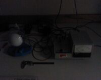
Constructed the circuit in the schematic (provided from notes of previous student P. Klimov).
started with no bias voltage. 5kv. filament began glowing immediately, waited approx 5 minutes to make sure filament was warm enough to sustain thermionic transmission of electrons.
Diffraction pattern was very difficult to see, in particular the inner diffraction ring was almost impossible to make out at anything less than 4800 volts, even running through multiple bias voltages. In fact increasing the bias voltage had the tendency to make the beam less intense and more difficult to see.
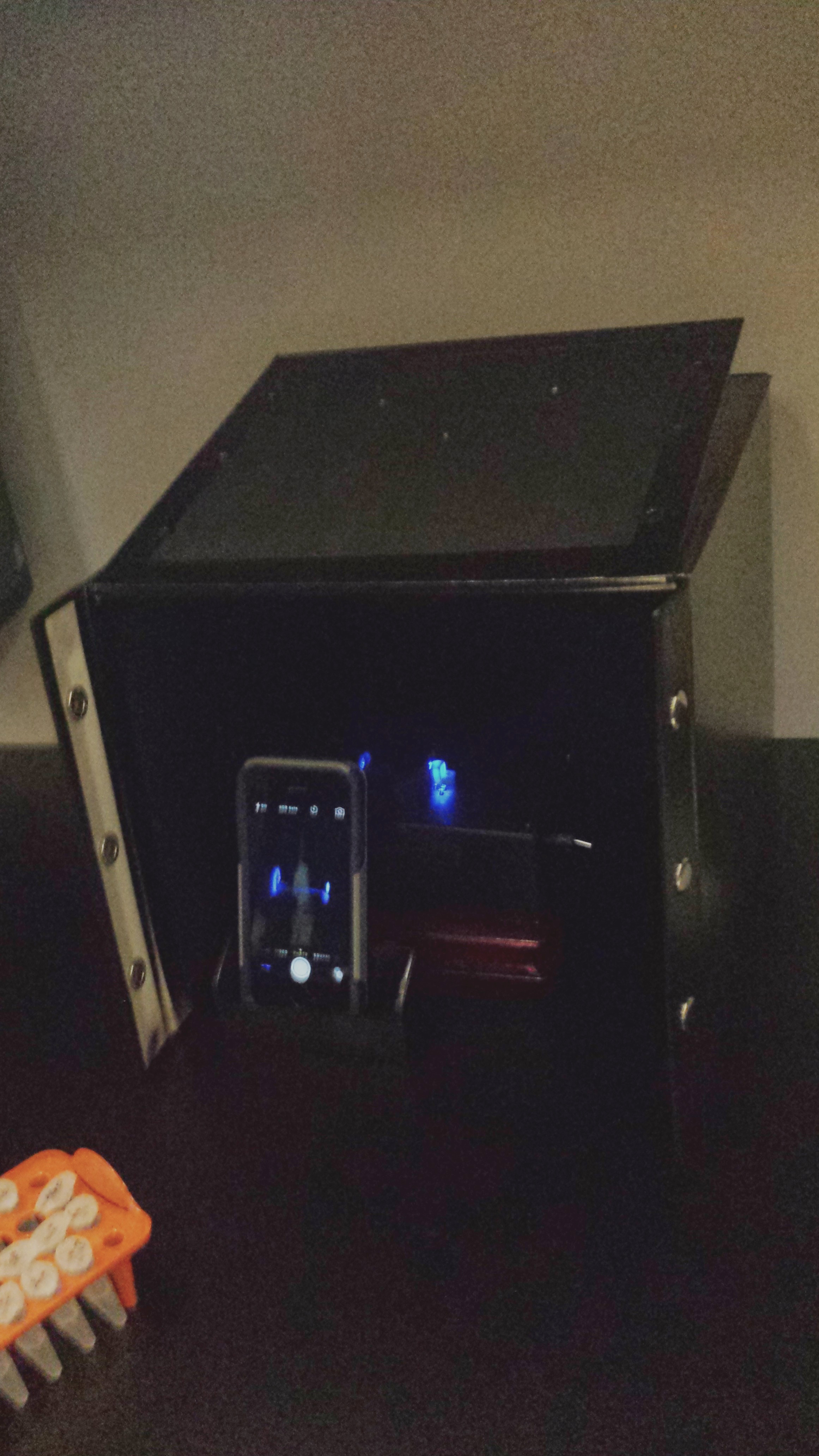
Included is a cellphone photograph of the lab setup:

need to figure out how to reduce pic in size, if you click on image you can see source file.
(Steve Koch 16:45, 11 October 2009 (EDT): I edited to show you two ways of making smaller)
data
values given for phototube
L=130.0±2mm
Glass thickness=1.5mm
radius of curvature=66.0mm
Week1
| V (V) | outer diameter (mm) | inner diameter (mm) |
|---|---|---|
| 5000 | 42.93 +/-1.5mm | 26.60 +/-1.5mm |
| 4900 | 44.96 +/-1.5mm | 27.12 +/-1.5mm |
| 4800 | 46.13 +/-1.5mm | 28.11 +/-1.5mm |
| 4700 | 49.24 +/-1.5mm | not visible |
| 4600 | xx | xx |
| 4500 | xx | xx |
| 4300 | xx | xx |
| 4200 | xx | xx |
| 4100 | xx | xx |
| 4000 | xx | xx |
| 3900 | xx | xx |
| 3800 | 49.94 +/-1.5mm | nv |
| 3700 | 49.94 +/-1.5mm | nv |
| 3600 | 50.86 +/-1.5mm | nv |
| 3500 | 52.87 +/-1.5mm | nv |
The Rings were difficult to see and measurements are more guesswork than fact as there was not a very good edge on any of the rings to use as a guide for where to place the caliper. Also the bias voltage setup is suspect as increasing the bias actually decreased the intensity of the beam. Ran into time constraints attempting to improve the visual quality of the rings and only took measurements at high and low end of the high voltage range. I need to assess the setup and circuit diagram to see what improvements can be made to get better performance from the electron beam in next weeks labwork.
Week2
During week two of data collection for this experiment I will flip the polarity of the bias voltage to see if there is an improvement in the visibility of the diffraction rings.
| V (V) | outer diameter (mm) | inner diameter (mm) |
|---|---|---|
| 5000 | 36.72 +/-1.5mm | NA |
| 4900 | 37.21 +/-1.5mm | N/A |
| 4800 | 37.78 +/-1.5mm v | 24.67 +/-1.5mm |
| 4700 | 38.11 +/-1.5mm | 25.02 +/-1.5mm |
| 4600 | 38.43 +/-1.5mm | 25.65 +/-1.5mm |
| 4500 | 38.96 +/-1.5mm | 26.59 +/-1.5mm |
| 4400 | 39.19 +/-1.5mm | 27.07 +/-1.5mm |
| 4300 | 39.39 +/-1.5mm | 27.52 +/-1.5mm |
| 4200 | 39.89 +/-1.5mm | 28.04 +/-1.5mm |
| 4100 | 40.08 +/-1.5mm | 28.27 +/-1.5mm |
| 4000 | 40.26 +/-1.5mm | 28.56 +/-1.5mm |
| 3900 | 40.41 +/-1.5mm | 28.81 +/-1.5mm |
| 3800 | 40.76 +/-1.5mm | 29.22 +/-1.5mm |
| 3700 | 41.01 +/-1.5mm | 29.63 +/-1.5mm |
| 3600 | 41.26 +/-1.5mm | not visible |
| 3500 | 41.56 +/-1.5mm | not visible |
Changing the polarity of the bias voltage improved the beam focus and seemed to give the effect I was looking for, removing some of the fuzziness of the rings, making the edges easier (still not easy) to take a measurement from. I also found the inner ring easier to see with the bias voltage at -15 volts while the outer rings were easier to pick up at about -2 volts on the bias voltage.
Raising the bias voltage to -15 volts while making the inner ring easier to see had the effect of limiting the output of the high voltage supply to a maximum of 4800 volts.
I Did find that extended running of the apparatus in the 4700V range and higher, after about 20 minutes the there seemed to be a discharge where the voltage would suddenly dip down to about 3500 volts and stay there until the voltage was taken below 3500 and then taken back up to the desired voltage. Not sure where that came from but it was a little disconcerting, possibly a safety feature kicking in or a sign that the power supply is unstable.
Error Analysis
The greatest source of systematic error was in the taking of the measurement itself. The appearance of the ring, the challenge of finding a clean edge of the ring, and the way that you are holding a flat vernier caliper up to a spherical surface put a strain on the idea that I could take a mesurement accurate to a hundredth of a millimeter.
The voltage output of the high voltage supply used an analog meter to display the output voltage rather than a digital meter so the high voltage reading could have been within a 100 volts plus or minus the actual value.
Results
SJK 17:04, 11 October 2009 (EDT)

I was able to open your excel sheet by changing extension to .xls. I noticed some good things, such as it looks like you've learned how to use the output array from LINEST: great! However, I also noticed a bunch of mistakes, which isn't good. First, you reversed axes on the outer diameter graph. Second, you reversed the X and Y's in LINEST, which means your slope was actually the reciprocal. I haven't gone further yet, but I suspect this is the reason your spacings are so far off. Here's a really good thing to do in the future: make sure to use the "trendline" feature on the graph, or somehow plot your best fit line through the data. If you'd done that here, you'd have noticed that the slope was not correct (that's how I discovered it, actually)
File:Elecdiff.xlsx(Steve Koch 16:51, 11 October 2009 (EDT): I changed file extension to *.xls and it seems to work for me: File:Elecdiff.xls)
  (having difficulty getting my excel file to open here, appears I have an older version of excel.
  Will use Matlab or newer version of excel next time.)
link to lab summary[[1]]
SJK 17:12, 11 October 2009 (EDT)

A really critical piece is missing here: I do not see mention of how you converted the best fit from LINEST into a lattice spacing. Although I can guess from above that you plugged in values into the equation you show, but you don't say that here, and your analysis sort of ends. Since you uploaded the excel spreadsheet anyway, you definitely should have included those calculations in excel!
