Sandbox: Difference between revisions
Replaced content with "{{Template:CHEM-ENG590E}} Dry etching is useful for materials and semiconductors that are chemically resistant and are not able to be wet etched." |
No edit summary |
||
| Line 1: | Line 1: | ||
{{Template:CHEM-ENG590E}} | {{Template:CHEM-ENG590E}} | ||
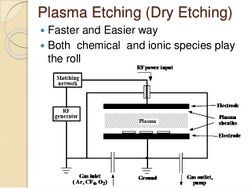
[[Image:Etching-7-638.jpeg|250px|right|thumbnail|'''Figure 1''' Depiction of plasma etching diagram with plasma between both electrodes removing substrate.]] | |||
'''Dry etching''' is the process of removing material by exposing the material to an ion bombardment to form a pattern. Unlike many wet etching techniques, dry etching is an anisotropic process, allowing for etching of flat, lateral walls. The process of dry etching is widely employed in microfabrication of circuitboards by etching of silicon substrates. | |||
==Mechanism== | |||
Dry etching is mostly driven by reaction of chemicals in plasma state. The plasma increases reactivity of chemicals, etching via a physical and chemical basis. Physical etching occurs from the bombardment of neutral particles while the chemical etching occurs from charged ions. | |||
A silicon substrate coated with an etching mask, with the etching mask leaving free the regions of the silicon substrate that are intended to be anisotropically etched, is subjected to a first etching step. | |||
For this purpose a mixture of SF6, SF2 and argon Ar can be used, which has a processing pressure between 10 and 100 μbar. The plasma generation is achieved with a microwave irradiation at outputs between 300 and 1200W (2.45 GHz). | |||
At the same time, a substrate for ion acceleration is applied to the substrate electrode. The substrate is typical 5-30V, and can be achieved with a high-frequency supply (13.56 MHz) at outputs between 2 and 10W. | |||
During the etching step, chemical reactive species and ions are generated in the reaction chamber aided by an electrical discharge sulfur and argon mix. | |||
[[Image:Silicon Etch Form.png|center|thumb|'''Figure 2''' Main reaction involved in etching at the Si surface.]] | |||
[[Image:Plasma Polymerization.png|center|thumb|'''Figure 3''' Plasma polymerization reaction occurring at the sidewalls.]] | |||
==Plasma Generation== | |||
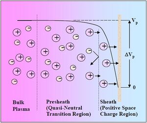
To perform dry etching the plasma must be generated first. The plasma is formed when electrons are accelerated to high energy states typically performed in high energy electric or magnetic fields using microwaves. The plasma contains positive ions, electrons, reactive chemical species, and neutral particles all contained in one bulk state. Without a plasma, all the processes involved in etching would occur at a higher temperature. There are different ways to change the plasma chemistry and get different kinds of plasma etching or plasma depositions. One of the excitation techniques to form a plasma is by using RF excitation of a power source of 13.56 MHz. Plasma etchers implement a form of plasma confinement to concentrate plasma into a region of the apparatus to allow control of etch rates and feature distribution. The plasma is confined by manipulating the properties of Debye sheaths which are transition layers between the plasma and solid. The Debye region is a result of the equilibrium formed from electrons bombarding the solid surface due to the higher electron temperature in comparison to plasma temperature, negatively charging it relative to the positive bulk plasma. This is tunable by adjusting the elecric or magnetic field applied across the electrode. | |||
[[Image:Debye Sheath.jpg|center|thumb|'''Figure 4''' A Debye sheath is shown above with clearly separated regions between bulk plasma and sheath layer.]] | |||
==Bosch Process== | |||
This process is a technique used to create high aspect ratio structures in silicon. It is able to etch defined features such as trenches, combs, and tongues anisotropically with a fair degree of selectivity in silicon substrate. The performance of this process, when done with microwave excitation (propagation ion etching) does not produce significant wall roughness. The Bosch process is widely used for obtaining smooth sidewalls required for industrial applications in electronics and circuit boards. The process involves successive etching and deposition cycles to coat the sidewalls as etching progresses. The process has been applied to the manufacture of flexible circuit boards, however deeper trenches for stretchable electronics required a titanium/gold bilayer hard mask. | |||
==Applications== | |||
Dry etching is useful for materials and semiconductors that are chemically resistant and are not able to be wet etched. | Dry etching is useful for materials and semiconductors that are chemically resistant and are not able to be wet etched. | ||
When used with photolithography, silicon dioxide can be applied or removed to trace paths for circuits for application in electronics. | |||
Dry etching is used in conjunction with photolithographic techniques to shape certain areas of a semiconductor surface to form wells in material for electrical contacts or circuit channels or to otherwise remove portions of semiconductor layers where vertical sides are desired. | |||
==References== | |||
#Plasma Potential & Sheath. (2018). Egloos.zum.com. Retrieved 24 February 2018, from http://egloos.zum.com/jinhwanlee/v/10888947 | |||
#Method of anisotropically etching silicon - Robert Bosch GmbH. (2018). Freepatentsonline.com. Retrieved 24 February 2018, from http://www.freepatentsonline.com/5501893.html | |||
#Ghoneim, M., & Hussain, M. (2017). Flexible Electronics: Highly Manufacturable Deep (Sub-Millimeter) Etching Enabled High Aspect Ratio Complex Geometry Lego-Like Silicon Electronics (Small 16/2017). Small, 13(16). http://dx.doi.org/10.1002/smll.201770089 | |||
#Rawat. (2018). Etching. Slideshare.net. Retrieved 24 February 2018, from https://www.slideshare.net/deepak10rawat/etching-55985755 | |||
#Plasma etching with a microwave cavity plasma disk source. (1989). Vacuum, 39(10), 997. http://dx.doi.org/10.1016/0042-207x(89)90957-3 | |||
Revision as of 21:00, 12 April 2018

Dry etching is the process of removing material by exposing the material to an ion bombardment to form a pattern. Unlike many wet etching techniques, dry etching is an anisotropic process, allowing for etching of flat, lateral walls. The process of dry etching is widely employed in microfabrication of circuitboards by etching of silicon substrates.
Mechanism
Dry etching is mostly driven by reaction of chemicals in plasma state. The plasma increases reactivity of chemicals, etching via a physical and chemical basis. Physical etching occurs from the bombardment of neutral particles while the chemical etching occurs from charged ions. A silicon substrate coated with an etching mask, with the etching mask leaving free the regions of the silicon substrate that are intended to be anisotropically etched, is subjected to a first etching step. For this purpose a mixture of SF6, SF2 and argon Ar can be used, which has a processing pressure between 10 and 100 μbar. The plasma generation is achieved with a microwave irradiation at outputs between 300 and 1200W (2.45 GHz). At the same time, a substrate for ion acceleration is applied to the substrate electrode. The substrate is typical 5-30V, and can be achieved with a high-frequency supply (13.56 MHz) at outputs between 2 and 10W. During the etching step, chemical reactive species and ions are generated in the reaction chamber aided by an electrical discharge sulfur and argon mix.


Plasma Generation
To perform dry etching the plasma must be generated first. The plasma is formed when electrons are accelerated to high energy states typically performed in high energy electric or magnetic fields using microwaves. The plasma contains positive ions, electrons, reactive chemical species, and neutral particles all contained in one bulk state. Without a plasma, all the processes involved in etching would occur at a higher temperature. There are different ways to change the plasma chemistry and get different kinds of plasma etching or plasma depositions. One of the excitation techniques to form a plasma is by using RF excitation of a power source of 13.56 MHz. Plasma etchers implement a form of plasma confinement to concentrate plasma into a region of the apparatus to allow control of etch rates and feature distribution. The plasma is confined by manipulating the properties of Debye sheaths which are transition layers between the plasma and solid. The Debye region is a result of the equilibrium formed from electrons bombarding the solid surface due to the higher electron temperature in comparison to plasma temperature, negatively charging it relative to the positive bulk plasma. This is tunable by adjusting the elecric or magnetic field applied across the electrode.

Bosch Process
This process is a technique used to create high aspect ratio structures in silicon. It is able to etch defined features such as trenches, combs, and tongues anisotropically with a fair degree of selectivity in silicon substrate. The performance of this process, when done with microwave excitation (propagation ion etching) does not produce significant wall roughness. The Bosch process is widely used for obtaining smooth sidewalls required for industrial applications in electronics and circuit boards. The process involves successive etching and deposition cycles to coat the sidewalls as etching progresses. The process has been applied to the manufacture of flexible circuit boards, however deeper trenches for stretchable electronics required a titanium/gold bilayer hard mask.
Applications
Dry etching is useful for materials and semiconductors that are chemically resistant and are not able to be wet etched. When used with photolithography, silicon dioxide can be applied or removed to trace paths for circuits for application in electronics. Dry etching is used in conjunction with photolithographic techniques to shape certain areas of a semiconductor surface to form wells in material for electrical contacts or circuit channels or to otherwise remove portions of semiconductor layers where vertical sides are desired.
References
- Plasma Potential & Sheath. (2018). Egloos.zum.com. Retrieved 24 February 2018, from http://egloos.zum.com/jinhwanlee/v/10888947
- Method of anisotropically etching silicon - Robert Bosch GmbH. (2018). Freepatentsonline.com. Retrieved 24 February 2018, from http://www.freepatentsonline.com/5501893.html
- Ghoneim, M., & Hussain, M. (2017). Flexible Electronics: Highly Manufacturable Deep (Sub-Millimeter) Etching Enabled High Aspect Ratio Complex Geometry Lego-Like Silicon Electronics (Small 16/2017). Small, 13(16). http://dx.doi.org/10.1002/smll.201770089
- Rawat. (2018). Etching. Slideshare.net. Retrieved 24 February 2018, from https://www.slideshare.net/deepak10rawat/etching-55985755
- Plasma etching with a microwave cavity plasma disk source. (1989). Vacuum, 39(10), 997. http://dx.doi.org/10.1016/0042-207x(89)90957-3
