20.109(F13): Mod 3 Day 3 TEM: Difference between revisions
No edit summary |
|||
| Line 4: | Line 4: | ||
=<center>TEM</center>= | =<center>TEM</center>= | ||
== | ==Today's Goal== | ||
Today we will be imaging our nanocomposites via TEM to confirm that our fabrication last week was successful. | |||
==Information gained via TEM== | |||
The Transmission Electron Microscope (TEM) enables 0.14 nm resolution by utilization of an electron beam over a light source found in optical microscopes. At this resolution, one can distinguish individual planes of atoms making TEM an excellent materials characterization instrument. As it is possible to visualize single atoms, one can use TEM to determine a slew of parameters which describe the structure of the material, such as crystal plane spacing. Additionally, TEMs can be equipped to perform energy-dispersive X-ray spectroscopy analysis (EDX/EDS/XEDS) or electron energy-loss spectroscopy analysis (EELS). The former, EDX, enables identification of the atomic composition of heavier elements in material. EDX has limited detection of elements below Na on the periodic table and no detection of elements below C on the periodic table. The latter, EELS, is the most sensitive to lighter elements, typically carbon to the 3d transition metals. EELS can reveal atomic composition, electronic properties of the valence and conduction band of a material, surface properties, and chemical bonding. | |||
Although we will be using TEM for materials characterization, it should also be noted that TEM is used for the analysis of biological materials as well. Since the electron beam passes through the sample that is being examined, the sample must be sufficiently thin and sufficiently sturdy to be hit by electrons in a vacuum. Rather than imaging single atoms, biological samples display contrast of components via different densities. Areas of higher density show up as a darker color than areas of low density, creating a “shadow ima | |||
==TEM function== | |||
The principle behind transmission electron microscopy is similar to the principles behind an optical microscope. Instead of light and glass lenses, however, the TEM utilizes an electron beam focused via electromagnetic lenses. Since the TEM utilizes an electron beam over visible light, the microscope must also function under a vacuum. This allows the electrons to remain traveling in a straight line as they have no air particles to collide with. | |||
Specifically, at the top of the column of a TEM, a high voltage electron beam is emitted by a cathode and focused via condenser lens. Then the beam is transmitted through the specimen. This image is then magnified through a series of electromagnetic lenses until it is recorded by a fluorescent screen or camera. | |||
==Sample preparation, using the TEM== | |||
We will be imaging our phage nanocomposites via TEM. To do this, we will first place samples on a TEM grid. TEM grids can be made of many kinds of materials. Each TEM grid design, however, includes lines of a conductive metal which disperses the electron beam and thereby prevents destruction of the sample from the harsh beam. Our TEM grids are composed of a copper mesh with carbon mesh is strung between the grids. Once a sample has been applied to our TEM grids, we will only visualize the portions of the sample contacting the carbon mesh, along with any imperfections in the carbon mesh itself. | |||
==Protocols== | ==Protocols== | ||
Revision as of 09:00, 6 November 2013

TEM
Today's Goal
Today we will be imaging our nanocomposites via TEM to confirm that our fabrication last week was successful.
Information gained via TEM
The Transmission Electron Microscope (TEM) enables 0.14 nm resolution by utilization of an electron beam over a light source found in optical microscopes. At this resolution, one can distinguish individual planes of atoms making TEM an excellent materials characterization instrument. As it is possible to visualize single atoms, one can use TEM to determine a slew of parameters which describe the structure of the material, such as crystal plane spacing. Additionally, TEMs can be equipped to perform energy-dispersive X-ray spectroscopy analysis (EDX/EDS/XEDS) or electron energy-loss spectroscopy analysis (EELS). The former, EDX, enables identification of the atomic composition of heavier elements in material. EDX has limited detection of elements below Na on the periodic table and no detection of elements below C on the periodic table. The latter, EELS, is the most sensitive to lighter elements, typically carbon to the 3d transition metals. EELS can reveal atomic composition, electronic properties of the valence and conduction band of a material, surface properties, and chemical bonding.
Although we will be using TEM for materials characterization, it should also be noted that TEM is used for the analysis of biological materials as well. Since the electron beam passes through the sample that is being examined, the sample must be sufficiently thin and sufficiently sturdy to be hit by electrons in a vacuum. Rather than imaging single atoms, biological samples display contrast of components via different densities. Areas of higher density show up as a darker color than areas of low density, creating a “shadow ima
TEM function
The principle behind transmission electron microscopy is similar to the principles behind an optical microscope. Instead of light and glass lenses, however, the TEM utilizes an electron beam focused via electromagnetic lenses. Since the TEM utilizes an electron beam over visible light, the microscope must also function under a vacuum. This allows the electrons to remain traveling in a straight line as they have no air particles to collide with.
Specifically, at the top of the column of a TEM, a high voltage electron beam is emitted by a cathode and focused via condenser lens. Then the beam is transmitted through the specimen. This image is then magnified through a series of electromagnetic lenses until it is recorded by a fluorescent screen or camera.
Sample preparation, using the TEM
We will be imaging our phage nanocomposites via TEM. To do this, we will first place samples on a TEM grid. TEM grids can be made of many kinds of materials. Each TEM grid design, however, includes lines of a conductive metal which disperses the electron beam and thereby prevents destruction of the sample from the harsh beam. Our TEM grids are composed of a copper mesh with carbon mesh is strung between the grids. Once a sample has been applied to our TEM grids, we will only visualize the portions of the sample contacting the carbon mesh, along with any imperfections in the carbon mesh itself.
Protocols
We're fortunate to have an expert from Angie Belcher's lab who will run the TEM grids you prepared. We've reserved the 2010FEG TEM, which is located in the basement of Bldg 24. Since the room that houses the instrument is small, we'll head over in our "supergroups," starting at about 1:30. The grids will take less than an hour to visualize and when you're not at the TEM, you should be working with your lab partner on your research proposal.
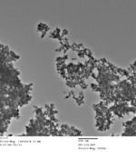
Here are some examples of the kinds of images you'll get at TEM today:


DONE!
For next time
REQUIRED ASSIGNMENT
Your team's research pre-proposal is due in lecture, M3D4. Please print out a copy of your wiki page as well as be prepared to show the page to the class and talk about it briefly. This is a great opportunity to get feedback and help with your ideas.
Next Day: Mod 3 Day 4: Solar Cell Assembly Previous Day: Mod 3 Day 2: Phage Nanowires